Intel will invest $3.5 billion in its Rio Rancho fab to support Foveros, its 3D manufacturing and packaging technology.
The site in New Mexico is currently used to manufacture Optane memory and Intel's embedded multi-die interconnect bridge (EMIB) and silicon photonics products.
The company also will spend $600m on expanding operations in Israel, home to its Mobileye subsidiary.
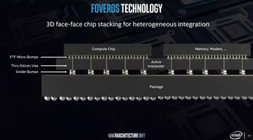
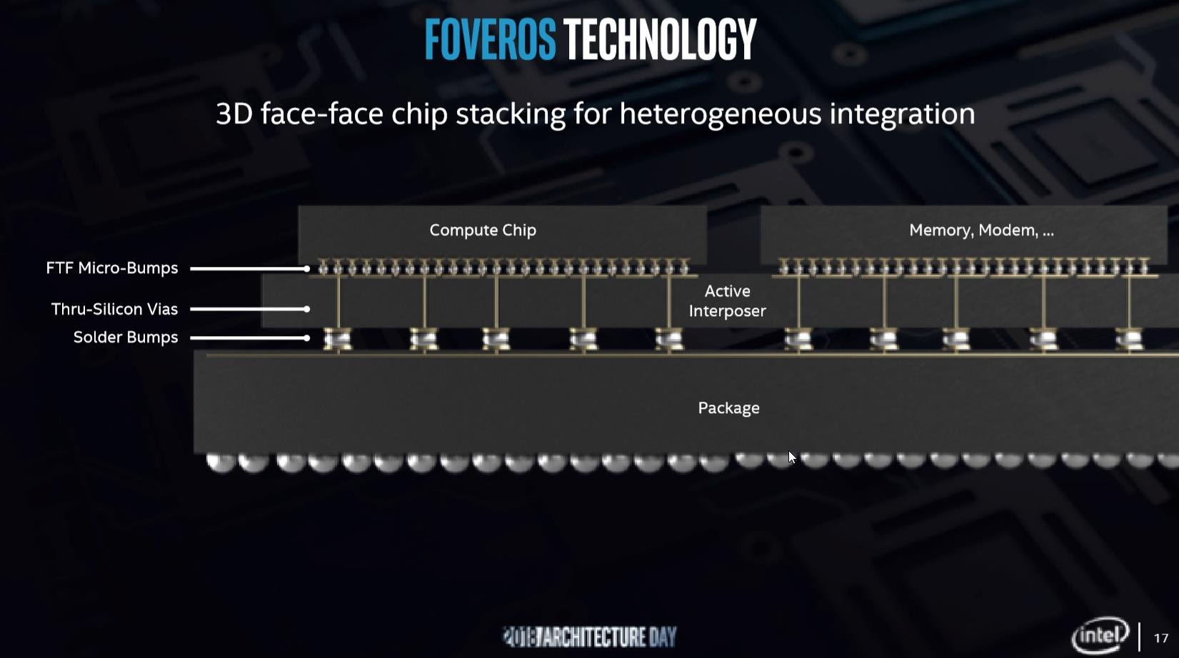
Foveros allows chiplets to be stacked virtually. Traditional chips have mostly relied on 'monolithic designs' where everything is on a single piece of physical silicon, making data management and chip design simpler.
Given the limitations of von Neumann architectures and slowing advances in x86 design, there has been a slow shift away from monolithic design to chiplets, where multiple pieces of silicon are connected to create a single processor.
The advantage is that each chiplet can be designed for a specific task, or it may be easier to create the individual chiplets rather than one massive monolithic piece of silicon. The chips can also be larger as they do not have to face the same limitations found with monolithic chips.
However, connectivity becomes an issue as the chiplets need to be able to communicate rapidly with each other to function.
AMD turned to chiplets for its highly successful Epyc server line, combining compute chiplets with a peripheral one.
The total die size of its server CPU is greater than what can currently be manufactured in a single monolithic design.
At Epyc's launch, Intel was highly critical of the concept of chiplets and criticized AMD's approach in on and off the record comments with media.
Facing a declining market share and years of delays in getting to 10nm (let alone 7nm) process node production, the company said it would turn to 3D stacking.
Instead of placing them on the same flat surface as AMD does, it would stack them on top of one another.
NAND and DRAM already use multilayer stacking, but Foveros is its own approach where multiple layers of high-performance compute are stacked together.
Currently, there is one Foveros product, the Lakefield CPU. It features on 10nm compute chiplet on top of a 22nm peripheral chiplet.
This reduced the surface area for the chip, making it suited for mobile and laptop markets. But critics have noted that the approach sacrificed performance and cost for a small amount of surface area, and said it was '2.5D stacking' rather than the full thing.
The company has since embraced the 2D chiplet form factor it criticized AMD for, with its core server chips set to use chiplets when it gets to 7nm.
At the same time, others are catching up on stacking technology. Rival manufacturer TSMC is building a plant for 2022 that will deploy its new 3D stacking technology, SoIC. The first customers will include Google and AMD.


