
Kurt Lender (Intel IO technology solution team strategist) summarizes the impact of chiplet technology by stating, “There is a reasonable expectation that HPC procurements over the next 10 years will leverage chiplet technology to better support their scientific workloads.” This expectation is reflected by other industry leaders, such as AMD’s Lisa Su (CEO, AMD) who answered “yes” when asked if she envisions HPC procurements over the next 10 years specifying custom chiplet designed computational chips rather than commodity off the shelf.
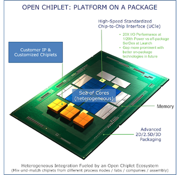
Chiplets introduce modular design into semiconductor fabrication and packaging. Think of this innovation as turning the silicon of the chip conceptually into the “motherboard” of a server. This silicon motherboard can accommodate custom compute, network, IO, and memory chiplet hardware optimized to best support application needs – and with the UCIe standard not be tied to one manufacturing process and/or vendor. It also opens the door to System on Package (SoP) designs that can potentially eliminate costly high pin count sockets and offers the potential for technology upgrades within the same socket via silicon packaging – a very exciting potential to leverage future supercomputer infrastructure investments along with disaggregated data centers. As will be discussed in this article, chiplet architectures also offer a pathway to zettascale (1021 flop/s) performance, the next three order of magnitude increase in HPC performance beyond exascale (1018 flop/s).
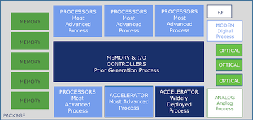
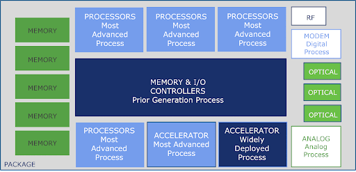
A high-level schematic illustrating the flexibility inherent in chiplet package design is shown below.
Lender notes the approach provides extraordinary power, performance, and time to market benefits. “It’s a new era”, he wrote in his blog, “of semiconductor architecture that puts designers in control and continues Moore’s vision of doubling computing power well into the foreseeable future.”
A three orders of magnitude impact on HPC
This new approach relies on extremely fast, and equally important, tested and verified chiplet silicon that can be incorporated and packaged into workload-optimized semiconductor devices.
Bespoke design means that HPC data centers can specify very dense, very close to the data compute devices that simply are not appealing or viable to market to the commodity-off-the-shelf (COTS) mass market. Such characteristics are necessary to achieve the next three orders-of-magnitude performance jump beyond exascale according to Intel’s Raja Koduri (Executive vice president and general manager of the Accelerated Computing Systems and Graphics Group at Intel Corporation).
An open bespoke chiplet ecosystem means that the HPC community will no longer be caught in the dilemma of the tail of the dog trying to wag the dog, where the body of the dog is the massive CPU and GPU COTS market. HPC just does not have the same economic clout as the mass market, so HPC designers are left to do the best they can. With a chiplet architecture, HPC architects can specify the bespoke hardware needs of their applications and pass those criteria off to the designers and the HPC vendors to get the best possible mix of compute, memory, and IO to support their workloads.
Open standards are key to zettascale HPC performance
An internal on-chip communication fabric is a key component that connects the chiplets to create a unified device on-chip and disaggregated data center off chip. The performance of this fabric is critical in achieving HPC and future zettascale (1021 flop/s) levels of performance.
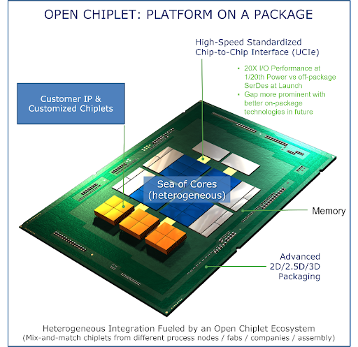
Major manufacturers are already using proprietary fabrics to connect on-silicon chiplets. They have recognized, via the UCIe 1.0 standard that an open standards approach is the path to an ecosystem where different process technologies – and chiplet designs from a multitude of companies - can be mixed-n-matched on silicon to address customer-specific compute, power, and density requirements. Current chiplet fabrication processes include 2D and 2.5D plus the very exciting and highly anticipated advent of 3D chip stacking manufacturing techniques.
Advanced packing technologies are all part of Intel’s new Integrated Device Manufacturing (IDM 2.0) strategy. According to Intel CEO Pat Gelsinger, IDM 2.0 is a major evolution of Intel’s IDM model.
New fabrication techniques means that a chiplet architecture can be adapted to deliver extreme performance and revolutionary power savings to the HPC community – far beyond what can be delivered by the COTS market. This explains why chiplets are an integral part of Intel’s zettascale strategy as expressed in Raja’s description of Intel’s Path to Zettascale
Raja points out that the communication fabric is particularly important as it gives designers the opportunity to minimize data movement and keep data close to the compute hardware. Both are very important to achieve the next three-order-of-magnitude performance jump to zettascale HPC supercomputers.
Even better, optical interconnects that can move HBM memory or other types of memory off the GPU/CPU package can be used, which, in turn, means that system designers can tie data directly to physically distant off-chip computing devices. These optical interconnects already exist such as the Ayar Labs TeraPHY in-package OIO chiplet and SuperNova laser light source.
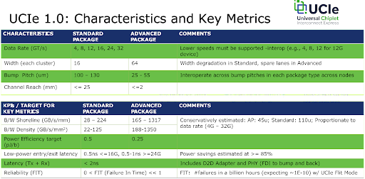
The UCIe characteristics and key metrics shown below clearly show that UCIe 1.0 specification is fast enough to support memory chiplets by providing sub 2 nanosecond (ns) transmit and receive latency and up to 32 Giga transfers per second (GT/s). Power, density, and other key measures are also included in the standard. According to the Intel slide shown below, the consortium believes the UCIe 1.0 has the necessary characteristics and key metrics to meet projected needs for the next 5-6 years.
The economics of bespoke HPC design
Lender notes that the cost for creating a UCIe-based chiplet design should be minimal. “Think of pricing like Compute Express Link (CXL). It will be minimal to get going.” After that, he notes that “there are a variety of scale-up and scale-out cost benefits that include the cost saving due to high-yields for the chiplets resulting from their smaller footprint compared to a monolithic silicon design, and the ability to specify high-density, high-power packages that can exploit HPC cooling capabilities. In its fullest expression, chiplet-based architectures give designers the ability to quickly integrate proven intellectual property (IP) designs and process technologies from multiple vendors into one package.”
Chiplets mean on-premises can outpace COTS HPC in the cloud
Translating all this into the tremendous cost and performance benefits that can be realized by the HPC community, Lender notes that “Chiplets do not burden the entire chip with moving quickly. This leads to faster and potentially lower cost design cycles.”
In other words, the advent of chiplet-based architectures may well be a defining moment in HPC systems design and procurement as bespoke chiplet designs can move quickly to provide power and performance envelopes for HPC systems that are unlikely to be matched by COTS hardware. This performance differentiation will be accelerated as designers incorporate the latest advances such as 3D chip stacking and other novel technology. Further, an expanding ecosystem of chiplets should reduce the challenges and compromises baked into hardware designed by single vendor design teams focused on a creating a corporate product line for the mass market.
UCIe has seismic implications for the data center
The implications are seismic for the HPC community as illustrated below by the on-chip and disaggregated usage models supported by UCIe both from a performance and infrastructure perspective.
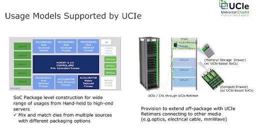
The flexibility in provisioning (shown on the right) supports amazing potential inherent in the UCIe v1.0 standard to upgrade existing infrastructure in the data center. It also supports the movement to zettascale by providing the ability to connect to off-package resources in the data center with on-chip performance.
Essentially, we can think of each Compute/Storage/Memory drawer in the illustration as the analogue of a rack containing many UCIe-based devices. Just as we can replace a rack of compute resources in a current data center to improve system performance, so can we replace one of the UCIe drawers containing newer, application optimized bespoke chips. The advance is that each chip can interact with memory and other compute devices in the compute drawer, just as if they are on-chip due to the speed and latency of a UCIe 1.0 compliant fabric.
Such an upgradable design means that data centers can look to incorporate fast and flexible upgrade cycles that reuse much of the existing power and cooling infrastructure investment while gaining access to the latest technology.
Accordingly, the vision of the UCIe consortium members is compelling. Upgradable HPC bespoke designs offer cost, feature, and performance benefits that are very exciting and can greatly exceed the performance of COTS designs. The indications are that chiplet-based architectures are going to be incorporated in some form into on-premises HPC investments over the next 10 years. It is likely this trend will continue far into the future.
Rob Farber is a technology consultant and author with an extensive background in HPC and in developing machine learning technology


