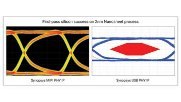
Synopsys has achieved first-pass silicon success using TSMC’s N2 process and certified digital and analog EDA (electronic design automation) flows for TSMC’s A16 and N2P technologies.
The company said the N2 achievement represents a “major step forward in the development of next-generation AI-enabled systems,” and the success will help accelerate the industry’s transition from FinFET to nanosheet architecture to help support increased chip performance and power efficiency.
While high-performance mobile SoC (system-on-chip) designs are leading the way in nanosheet adoption, the transition is also being driven by the growing demand for Edge AI and mobile computing, with the company noting that on-device AI models are currently limited to less than 10 billion parameters due to performance, heat, and power issues associated with trying to run complex Mixture of Experts (MoE) models and AI agents on mobile and Edge devices.
However, Synopsys said next-generation designs will be able to make use of advances in memory and storage technologies, in addition to the interfaces that connect them, with nanosheet transistor architecture necessary to support continued device scaling and reducing leakage, while increasing chip performance and power efficiency.
Synopsys and TSMC have collaborated for more than 20 years, with Synopsys stating that the first-pass success on TSMC’s 2nm technology with nanosheet transistor structure demonstrates the “strengths and innovation” of the two organizations’ longstanding partnership.
The partnership has also seen the two companies announce the delivery of EDA and IP solutions for TSMC's advanced processes and advanced packaging technologies to accelerate AI chip design and 3D multi-die design innovation.
This includes the availability of certified digital and analog flows on TSMC A16 and N2P processes and the initial development of EDA flows on TSMC's A14 process. The two organizations are also working on the tool certification for the newly announced TSMC N3C technology, building on the available N3P design solutions.
The Synopsys 3DIC Compiler has also been certified by TSMC, further accelerating semiconductor design for ultra-high-density 3D stacking by supporting 3Dblox and enabling TSMC's CoWoS technology with 5.5x-reticle interposer sizes.
"Synopsys and TSMC are helping the semiconductor industry speed up the pace of innovation for Angstrom-scale designs by providing mission-critical EDA and IP solutions optimized for the most advanced process technologies," said Sanjay Bali, SVP of strategy and product management at Synopsys. "Together, we are delivering future-ready solutions that empower engineers to push the boundaries of technology, achieve their design goals, and bring their products to market faster."
Lipen Yuan, senior director of advanced technology business development at TSMC, added: “Collaborating closely with our Open Innovation Platform (OIP) design ecosystem partners like Synopsys is vital to enable our mutual customers with certified flows and high-quality IP that are essential to meet or exceed their design targets on TSMC's advanced processes."


