
Dutch chipmaking equipment company ASML has said it will deliver a EUV (extreme ultraviolet) lithography system that offers 50 percent more light power, improving wafer output, by the end of the decade.
Featuring a 1,000W light source, the future system would allow companies to process up to 330 wafers an hour, up from 220 at present, helping to reduce semiconductor manufacturing costs, the company told Reuters in an interview published earlier this week.
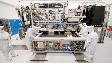
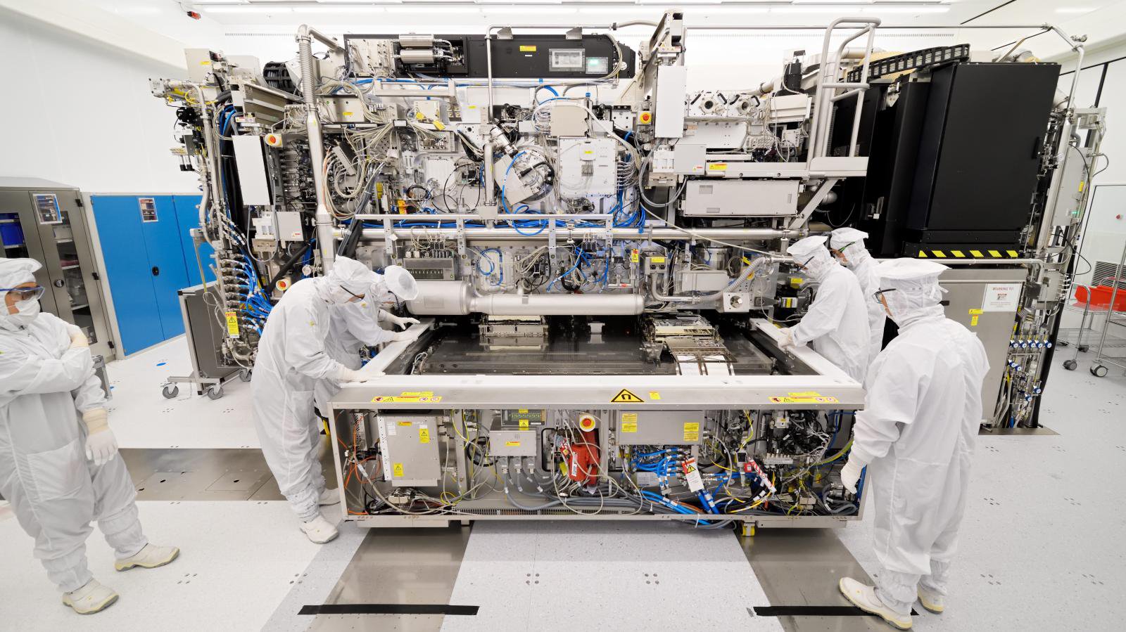
EUV lithography works by using a 13.5nm light to print nanometer-sized transistors on silicon wafers. According to ASML, the EUV light source is generated by a laser system that fires tin droplets 50,000 times per second, vaporizing them into a plasma that emits the required light. Currently, ASML’s lithography machines are powered by a light source totaling 600W.
In order to achieve the increased yield ASML is touting, the 1,000W light source will be equipped with a laser system capable of firing 100,000 tin droplets per second and shaped into plasma via two smaller laser bursts, as opposed to the current single shaping burst. However, a spokesperson from ASML separately told Tom’s Hardware that technology is currently under development and it would be years before it is commercialized.
Despite this, ASML believes that once it has reached the 1,000W benchmark, further advancements will be easier to achieve. “We see a reasonably clear path toward 1,500W, and no fundamental reason why we couldn't get to 2,000W,” Michael Purvis, ASML's lead technologist for its EUV source light, told Reuters.
ASML is the sole global supplier of extreme ultraviolet lithography machines, although in recent years, a number of companies have sought to challenge its dominance by developing more cost-efficient or alternative approaches to lithography technology.
In August 2024, Japanese scientists published a simplified lithography method that they claim consumes less than one-tenth the power of conventional EUV lithography machines. That same year, Canon shipped its first nanoprint lithography machine to the Texas Institute for Electronics (TIE), touting the FPA-1200NZ2C tool as a low-cost alternative to ASML’s photolithography technology.
In October 2025, US startup Substrate claimed it had developed a chipmaking tool that can compete with the advanced lithography tools manufactured by ASML. Two months later, the US government has agreed to invest $150 million in chip lithography startup xLight in exchange for an undisclosed equity stake.


Comments