
The University of Southampton has opened the first electron-beam (e-beam) lithography facility in Europe to support next-generation semiconductor design.
The facility will form part of the British university’s Optoelectronics Research Centre (ORC), which oversees research in photonics and optoelectronics.
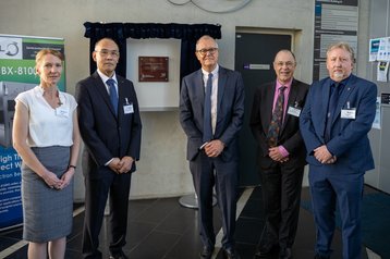
E-beam lithography uses a focused beam of electrons to create patterns in materials that are too small to fabricate with conventional photolithography.
The facility is the second of its kind in the world, and the first to exist outside of Japan.
The center was opened the same week that the UK government announced a £4.75 million ($6.7m) package to fund new bursaries, chip design courses, and school outreach to address the country’s semiconductor skills gap.
According to the UK government, the chip industry is expected to contribute an estimated £10 billion ($13bn) to our economy each year, with the sector projected to grow to an estimated £17bn ($23bn) by 2030.
“Britain is home to some of the most exciting semiconductor research anywhere in the world – and Southampton’s new E-beam facility is a major boost to our national capabilities,” said Science Minister Lord Vallance.
"By investing in both infrastructure and talent, we’re giving our researchers and innovators the support they need to develop next-generation chips right here in the UK.“
In October 2024, the UK government acquired a gallium arsenide chip fab in the English town of Newton Aycliffe, County Durham.
In March of that same year, the government also cleared US electronics company Vishay’s takeover of Newport Wafer Fab - the UK’s largest semiconductor manufacturing site, located in South Wales.






Comments