Malaysia is planning to build the largest integrated circuit design park in Southeast Asia to promote domestic semiconductor design, prototyping, and manufacturing.
The Malaysian government will offer a number of incentives, including tax breaks, office space subsidies, and visa exemption fees, to attract tech companies and investors to the facility.

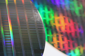
Currently, around 13 percent of global chip testing and packaging takes place in the country but the government reportedly wants to further establish the country as a leader in semiconductor front-end design.
The Malaysia Semiconductor Accelerator and IC Design Park will be housed in Puchong, in the state of Selangor. The site will initially be located in a 45,000 sq ft building, which will be expanded to a 60,000 sq ft site at a later date.
In comments reported by the Malay Mail, Yong Kai Ping, CEO of the Selangor Information Technology and Digital Economy Corporation (Sidec), said the site is expected to become operational in July and has already seen “strong demand from international investors.”
He added that the site will provide career opportunities for people in the region, employing more than 300 IC design engineers in the first year of operation and offering high salaries for such roles.
According to the Malay Mail, the park is expected to bring in economic returns of RM500 million to RM1 billion ($105-210m).
In addition to the capital put forward by the government, Khazanah Nasional - Malaysia's sovereign wealth fund - will also launch an investment fund to support high-growth Malaysian companies, with an initial allocation of RM1 billion.


