Intel has separated its Product and Foundry lines into two separate businesses.
As a result of the move, Intel Foundry Services has been rebranded as simply Intel Foundry, with the business expanding to include technology development, supply chains, fabrication, and packaging services. Intel's Product division will now focus its efforts on product development alongside licensing client, desktop, and networking solutions.

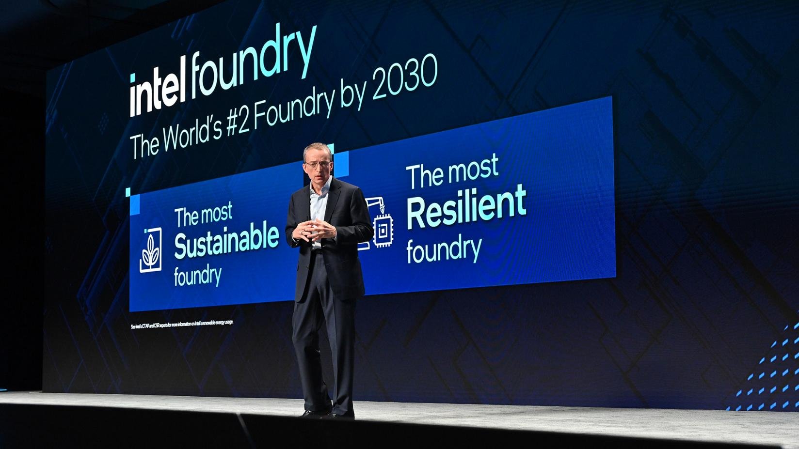
The announcements were made yesterday (February 21) at Intel’s first foundry event, Intel Foundry Direct Connect in San Jose, California.
According to Stuart Pann, SVP and general manager of what was IFS, the two new organizations will be legally distinct entities, with their own staff and processes to ensure customer confidentially.
Intel updates its process roadmap
In addition to announcing the business spinouts, Intel unveiled an extended process technology roadmap while confirming that its five-nodes-in-four-years (5N4Y) strategy remained on track. The 5N4Y plan will see Intel Foundry release a new node every two years, adding node evolutions along the way, with each successive node offering a significant increase in performance-per-watt.
Intel 3, the next node on the roadmap, is now ready for high-volume manufacturing, with the new generation of Xeon server CPUs set to be the first product to include the Intel 3. Code-named Sierra Forest, the server CPUs are expected to launch in the first half of this year.
Intel also plans to extend the node further this year, developing an Intel 3-T that will use Foveros Direct to connect chips with a technology known as through-silicon vias. Instead of using solder connections which slow down data transfer, Foveros Direct uses direct copper-to-copper connections that result in lower latency and higher bandwidth, while reducing the die area necessary for communication.
Meanwhile, with an anticipated availability date of 2027, the newly announced Intel 14A will have transistors carved into it using the High-NA extreme ultraviolet (EUV) lithography scanner that ASML recently delivered to Intel.
The company’s final two nodes, Intel 20A and Intel 18A, have an expected manufacturing date of later this year.
Intel has invested heavily in expanding its chip manufacturing capacity in recent years, plowing $20 billion into a semiconductor fabrication plant in Columbus, Ohio, and an additional $47bn across sites in Arizona, Germany, and Malaysia.
However, the projects have not been without their issues, with the company having to push back its construction timetable at the Ohio fab earlier this year, citing market challenges and the slow rollout of funding from the US government.
Intel strikes custom chip manufacturing deal with Microsoft
Another major announcement to emerge from the event was a $15 billion deal with Microsoft which will see Intel produce Microsoft-designed custom chips for the company using Intel’s 18A process.
“We are in the midst of a very exciting platform shift that will fundamentally transform productivity for every individual organization and the entire industry,” said Microsoft CEO, Satya Nadella. “To achieve this vision, we need a reliable supply of the most advanced, high-performance, and high-quality semiconductors. That’s why we are so excited to work with Intel Foundry, and why we have chosen a chip design that we plan to produce on Intel 18A process.”
Although no information was given regarding the specifications of the custom chips, earlier this week, it was reported that Microsoft is developing its own networking card in an effort to reduce the company’s reliance on Nvidia hardware.
Microsoft has also developed its own line of in-house Arm CPU and AI accelerator chips for use on Azure.


