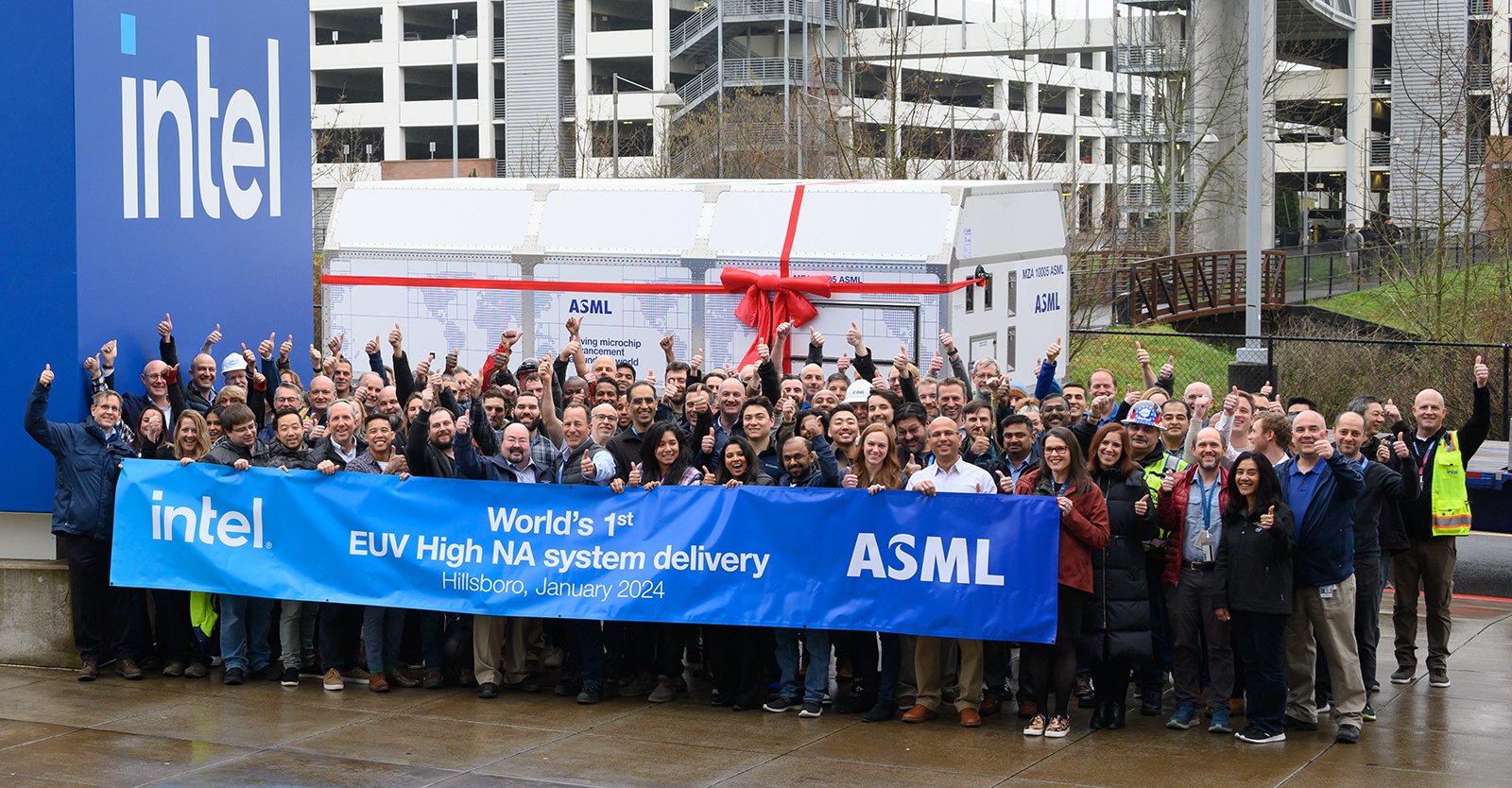
ASML has delivered a first-generation Twinscan EXE:5000 High-NA extreme ultraviolet (EUV) lithography scanner to Intel, seven years after Intel first ordered the machine.
The High numerical aperture (High-NA) scanner will be assembled by the two companies in the coming months. The machine is capable of producing more than 200 wafers per hour and the technology is expected to be mass produced and inserted into Intel’s post-18A node sometime in 2025.

The machine was shipped by ASML on December 21 and Intel announced on January 4 that it had finally arrived at the company’s Oregon plant via a post on X, formerly known as Twitter.
ASML is the sole supplier in the world of extreme ultraviolet lithography (EUV) photolithography machines and High-NA EUV lithography tools provide a significant improvement on current EUV tools as they are capable of 8nm resolution rather than the traditional 13nm.
Consequently, these next-generation High-NA EUV scanners are expected to play an important role in the manufacturing of 3nm chips and could reduce complexity, enhance yields, and reduce costs by removing the need for EUV double patterning from the process.
Speaking in 2022, when Intel first announced its plans to deploy High-NA technology, Dr. Ann Kelleher, executive vice president and general manager of Technology Development at Intel said: “Intel’s focus is to stay at the forefront of semiconductor lithography technology and we’ve been building our EUV expertise and capacity over the last year.
“Working closely with ASML, we will harness High-NA EUV’s high-resolution patterning as one of the ways we continue Moore’s Law and maintain our strong history of progression down to the smallest of geometries.”


