
GlobalFoundries (GF) has been awarded an additional $9.5 million in US federal government funding to advance the manufacturing of gallium nitride-on-silicon (GaN-on-Si) chips at its fab in Essex Junction, Vermont.
The funding was awarded to the company by the US Department of Defense’s Trusted Access Program Office (TAPO).
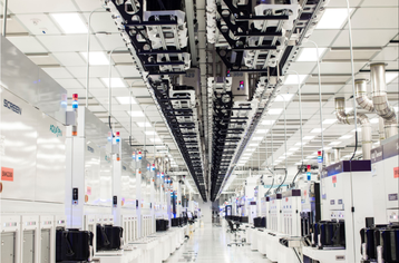
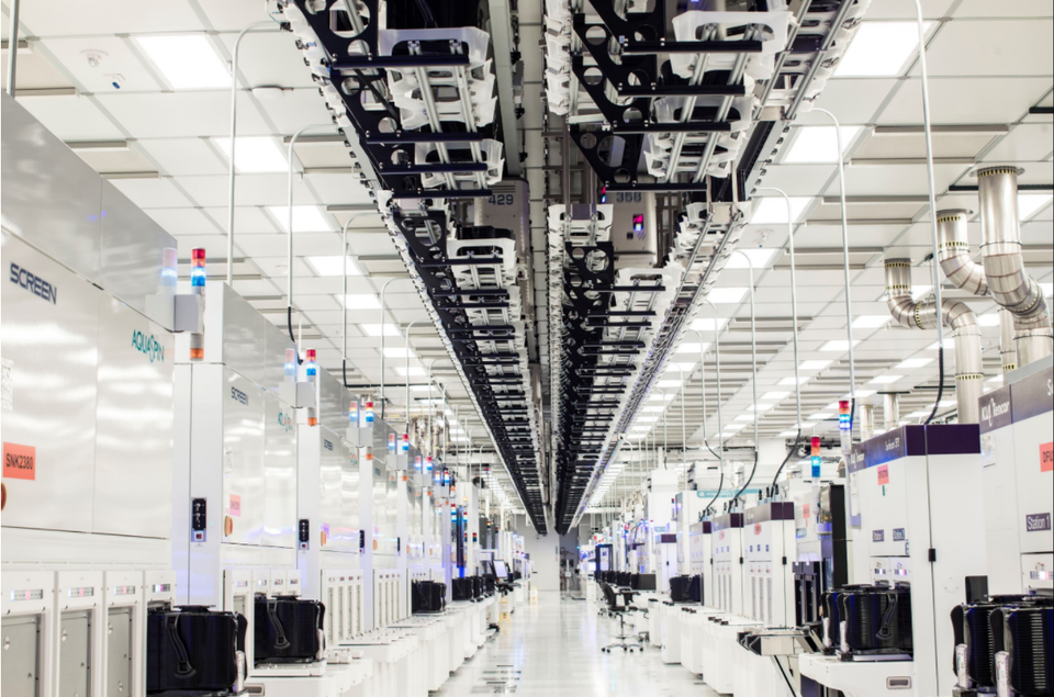
In a statement, GF said the funds will allow the company to add new tools, equipment, and prototyping capabilities, taking it one step closer to achieving full-scale manufacturing of its 200mm gallium nitride (GaN) chips in the state.
GaN is a wide-bandgap material and can handle higher amounts of power than silicon. As a result, GaN-based chips can be more efficient and durable than their silicon counterparts and are becoming more widely used across various industries, particularly for power electronics applications.
In July 2024, GF acquired Tagore Technology’s gallium nitride IP portfolio for an undisclosed amount.
“GF is proud of its leadership in GaN chip technology, which is positioned to make game-changing advances across multiple end-markets and enable new generations of devices with more energy-efficient RF performance and faster-charging, longer-lasting batteries,” said Nicholas Sergeant, VP of IoT and aerospace and defense at GF, adding that “realizing full-scale GaN chip manufacturing will be a catalyst for innovation, for both our commercial and government partners, and will add resilience and strengthen the semiconductor supply chain.”
The announcement comes a month after GlobalFoundries finalized the negotiations for its CHIPS and Science Act funding, under which it will receive $1.5 billion in direct funding to expand its manufacturing capabilities in New York and Vermont.
The company, which was one of the first to be awarded US CHIPS Act funding, is also set to receive more than $550 million in support from the New York State Green CHIPS Program.
GlobalFoundries signs deals with Icsense and Soitec
Elsewhere last week, GlobalFoundries revealed it had signed foundry agreements with ICsense and Soitec to boost application-specific integrated circuit manufacturing and radio frequency silicon on insulator (RF-SOI) substrates.
The agreement with ASIC specialists ICsense will see the latter have access to GF’s manufacturing capabilities and industry partners, allowing for quicker market launches of custom ICs whilst simultaneously providing early access to new design and process data.
Meanwhile, the deal with French engineered substrate manufacturer Soitec will see the company deliver 300mm RF-SOI substrates to GF for the production of the chipmaker’s most advanced RF solution, 9SW.
RF-SOI-engineered substrates are required for 5G, 5G-Advanced, WiFi, and other smart mobile device radio frequency front-end (RFFE) modules. According to GF, its 9SW platform delivers significant reduction in active and standby power consumption, providing an efficiency enhancement of more than 20 percent through lower on-resistance and off-capacitance figures of merit.
“Soitec has established the world's largest production capacity to meet growing demand for advanced RF-SOI substrates supporting 5G and WiFi technologies in smartphones, as well as future AR-VR and IoT devices,” says Jean-Marc Le Meil, Soitec’s executive VP for mobile communications.
“We are delighted to extend our longstanding relationship with GlobalFoundries in developing the next generation of 300mm RF-SOI technologies. The transition from 5G to 5G-Advanced, and eventually 6G, requires ever-higher performance and energy efficiency, as well as increasing compactness for next-generation devices.”






Comments