
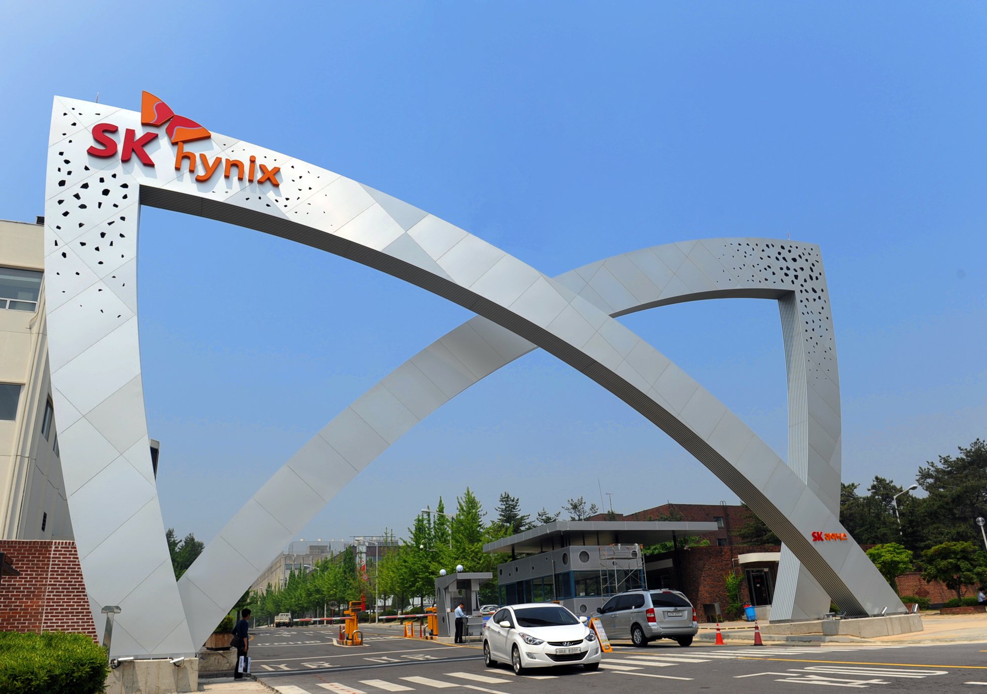
SK Hynix is planning to build a new back-end production facility in Cheongju, South Korea.
Citing messages posted to an internal bulletin board, The Korea Herald reported that the facility, dubbed P&T 7, will be located on the site of a former LG factory.
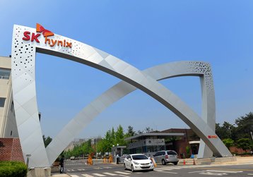
The memory chip maker has reportedly already begun demolition at the site, with the old factory expected to be fully cleared by September 2025. SK Hynix currently has six P&T (packaging and testing) facilities in Icheon and Cheongju, South Korea.
In addition to providing packaging and testing capabilities, the report noted that P&T 7 will also serve as a test fabrication site, although the timeline for construction of the facility has yet to be decided.
“The role of back-end processes in memory semiconductors is becoming increasingly important as they add significant value beyond traditional manufacturing,” an SK Hynix official told The Korea Herald. “The company seeks to improve its packaging technology.”
SK Hynix is also constructing P&T fabs outside of South Korea, announcing in April 2024 plans to invest $3.87 billion to build an advanced chip packaging facility in the US at West Lafayette, Indiana. That facility will produce next-generation high bandwidth memory (HBM), the highest-performing Dynamic Random Access Memory (DRAM) chips that can be used in GPUs to train AI models.
In December 2024, the company was awarded $458 million in direct funding under the CHIPS and Science Act to support construction of the facility.




Comments