
Photonic computing company Lightmatter has claimed an eight-fold jump in wavelength density, with potential implications for handling AI data center demands.
In what it claimed to be an industry first, the firm demonstrated a bidirectional dense wavelength division multiplexing (DWDM) link carrying 16 independent wavelengths over a single strand of standard single-mode fiber (SMF).
Linking two chips in traditional AI networks usually requires at least two separate optical fibers, one for each traffic direction. Lightmatter claimed to have used a single fiber, delivering an aggregate 800 Gbps–400 Gbps in each direction, across a 1km (0.6 mile) distance, with each channel operating at 50 Gbps.
Tests saw an eight-fold improvement in wavelength density compared with current two-wavelength – or lambda (λ) – bidirectional (BiDi) links.
“This BiDi advancement doubles the radix (the number of I/O ports) and bandwidth density as compared to existing CPO solutions without increasing the fiber count,” Lightmatter founder and chief scientist Darius Bunandar, PhD, wrote in a summary of the demo.
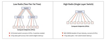
“A higher radix… reduces the number of hops a data packet must take to cross the network. Fewer hops mean fewer switches are needed for a given bisection bandwidth – enabling lower hardware costs and reduced power consumption.”
This could potentially mean more bandwidth density at a lower cost for data center operators in the era of AI.
Photonic tech is seeing a major impact on bandwidth, size, and energy efficiency, with recent Ciena research reporting AI workloads will place the biggest demand on data center interconnect (DCI) bandwidth in the next two to three years.
Details of the demo
Bunandar detailed that the DWDM link was centered on the 1310nm band, with eight odd-numbered wavelengths in the 1310nm window in one direction interleaved with eight even-numbered wavelengths in the other.
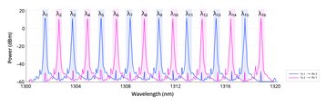
“We use a high-density arrangement that features 400GHz spacing between channels going the same way and a tight 200GHz spacing between adjacent transmit and receive channels,” Bunandar explained.
Lightmatter claimed the breakthrough relied on its closed-loop digital control system that counters thermal drift, a problem with temperature-sensitive micro-ring modulators (MRMs), with eight used in total to encode data.
The closed-loop stabilization ensures “a continuous, low-error transmission even as the chip’s junction temperature fluctuates," according to Bunandar.
A three-dimensional stacked co-packaged-optics (3D CPO) stack built on Lightmatter's Passage L200 chip helped polarization-insensitivity, ensuring constant performance no matter the orientation of the light’s electric field.
Such stacks see a silicon-photonics engine directly beneath or above the host ASIC, meaning electrical signals are converted to light within microns of the compute core. This can enable higher bandwidth and lower input/output (I/O) power than traditional pluggable optics.
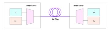
“The photonics (MRMs, photodetectors), all analog front-end circuitry, the Tx (transmitter) drivers, and the Rx (receiver) transimpedance amplifiers are all fabricated monolithically on a single chip,” added Bunandar on the overall architecture.
The Passage L200 is the first commercial SKU built on Lightmatter’s photonics engine. April saw the company release two new models designed to tackle the bandwidth bottlenecks associated with increasingly dense AI deployments.
Last fall saw Lightmatter valued at $4.4 billion in a $400 million funding round that saw participation from Google Ventures and others.
The company holds manufacturing partnerships with GlobalFoundries, ASE, and Amkor.
In January of this year, Lightmatter joined the Ultra Accelerator Link (UALink) Consortium, with the aim of standardizing advanced interconnect solutions for large numbers of AI accelerators, offering its Passage interconnect solution.






Comments