
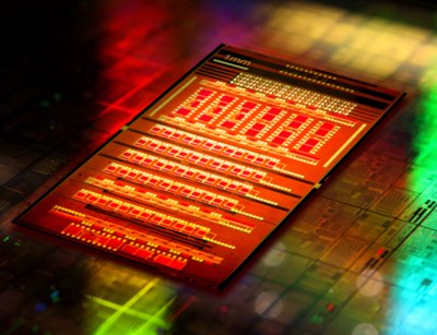

Scientists at IBM have rounded off a decade of development with a new technology they say integrates electrical and optical devices on the same piece of silicon, the outcome being computer chips that can communicate using pulses of light.
The development removes the need to use electrical signals and can result in smaller, faster and more power-efficient chips that those traditionally used, according to IBM.
IBM Research Science and Technology VP Dr TC Chen said the CMOS Integrated Silicon Nanophotonics will further IBM's supercomputing program Exascale, which it is using to develop technologies to develop a supercomputer that it says will one day perform one million trillion calculations (Exaflops) in a single second ÔÇô 1,000 times faster than any computer today.
"The development of the Silicon Nanophotonics technology brings the vision of on-chip otical interconnects much closer to reality," Chen said. "With optical communications embedded into the processor chips, the prospect of building power-efficient computer systems with performance at the Exaflop level is one step closer to reality."
IBM said the new chip technology can allow for a ten-fold increase on improvement in integration density when it comes to current manufacturing techniques and can be produced on the front-end of a standard CMOS manufacturing line, without the need for special tooling. It uses a suite of ultra-compact active and passive silicon nanophotonic devices that are scaled down to the diffract limit, according to IBM Research Silicon Nanophotomics Department manager Dr Yurri A Vlasov.
"The CMOS Integrated Nanophotonics breakthrough promises unprecedented increases in silicon chip function and performance via ubiquitous low-power optical communications between racks, modules, chips or even within a single chip itself," Vlasov said. "The next step in this advancement is to establish manufacturability of this process in a commercial foundry using IBM deeply scaled down CMOS processes."
The current CMOS fabrication flow only needs a few more processing modules than is currently used, according to Vlasov.