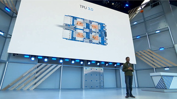
At its annual I/O conference, Google unveiled the latest generation of its Tensor Processing Unit, TPU 3.0.
Due to the high power density of the hardware, the application-specific integrated circuit (ASIC) will be liquid cooled - a first for the search and advertising giant. The company expects to begin large scale deployments within a few months.
Feeling the heat
“These chips are so powerful that, for the first time, we’ve had to introduce liquid cooling in our data centers,” Google CEO Sundar Pichai said.
“And we’ve put these chips in the form of giant pods. Each of these pods is now eight times more powerful than last year’s [TPUs], well over 100 petaflops. This is what allows us to develop better models, larger models, more accurate models, and helps us tackle even bigger problems.”
Google did not, however, share the benchmark used to claim 100 petaflops performance. The original TPU was very limited in the range of applications it could be used for, had no support for branch instructions, and was primarily applied to machine learning inferencing tasks. TPU 2.0 brought support for machine learning training and execution, with 64 chips in an eight-rack pod providing up to 11.5 petaflops.
“For a while we’ve been investing in the scale of our computational architecture,” Pichai said. “[The TPUs] are driving all the product improvements you’re seeing today, and we’ve made it available to our cloud customers.”
Each TPU 3.0 has 128 GB of high-bandwidth memory, twice the memory of its predecessor. Further specifications of the architecture were not provided, nor were the finer details of the liquid cooling process.
Images of a TPU motherboard appear to show direct-to-chip liquid cooling, with four chips on each board, and coolant delivered to copper cold plates above each ASIC.
With AI and machine learning workloads becoming increasingly important, high density racks are likely to become more popular, along with liquid cooling solutions that deal with the large amounts of heat they produce.

