Google has trained a machine-learning system to place elements in a microchip design - and it does it much better and faster than its human colleagues, saving space and power, while improving performance.
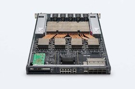
The company is already using the technique to place memory blocks in production chips such as its tensor processing units (TPUs). This week the science journal Nature published a paper on the use of graph placement for so-called "floorplanning" of chips, by a team led by Azalia Mirhoseini.
In an opinion article, Nature said that automating chip design could speed future hardware generations, but warned: This is an important achievement and will be a huge help in speeding up the supply chain, but the technical expertise must be shared widely to make sure the ‘ecosystem’ of companies becomes genuinely global. And the industry must make sure that the time-saving techniques do not drive away people with the necessary core skills.
For breaking data center news, features, and opinions, subscribe to DCD's newsletter

Better chips by design
Silicon chips are constructed from multiple components, but "floorplanning," or designing the physical layout is a complex task. Google showed its AI system 10,000 designs, evaluated for efficiency and performance. After six hours, the AI was able to design ships as well or better than humans could after months of work.
The AI was set up to approach the problem as a game in which it placed pieces on a board to achieve a winning result. The game comparison is instructive: while the game of Go has some 10360 configurations (its "state space"), a chip can have a state space of 102,500 - making this more than 102000 more complex.
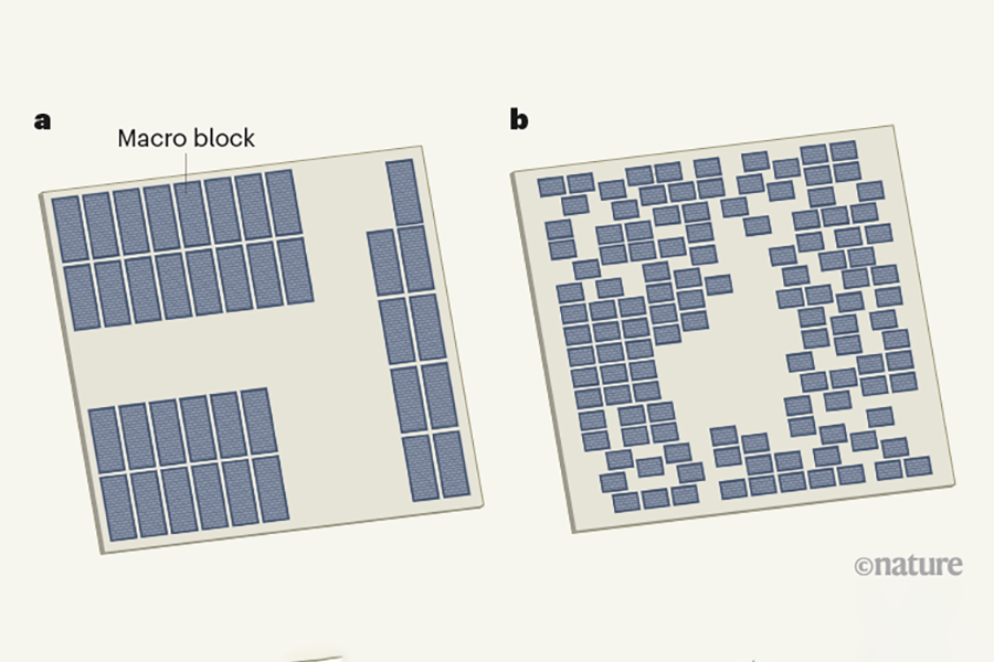
The system placed large units or "macro blocks" first, filling in the space around them with smaller cells - and the results look somewhat surprising. The diagram, developed from the paper published in Nature, shows the placement of macro blocks for memory. In a, the Ariane RISC-V processor designed by humans, macro blocks are neatly lined up leaving space in between for smaller components. In b, Google's AI improved performance and allowed better placement of all the cells involved by rearranging and grouping the memory blocks differently.
The paper was first shown as a pre-print on the Arxiv site last year, and Google's AI head Jeff Dean described it in a keynote speech at the International Solid-State Circuits Conference in February 2020. Following that, Google revealed the technique has been used in chip developments such as the design of recent tensor processing units (TPUs).
"Our method was used to design the next generation of Google’s artificial intelligence (AI) accelerators, and has the potential to save thousands of hours of human effort for each new generation," say the authors in their abstract. "Finally, we believe that more powerful AI-designed hardware will fuel advances in AI, creating a symbiotic relationship between the two fields."

