
"I would say 2026/27 will really be when we see GaN ramp into mass production,” proclaims Antoine Jalabert, vice president, GaN division at semiconductor supplier Onsemi.
“When you look at Nvidia’s roadmap, there’s no other way than to use GaN that will allow you to reach those kinds of power densities.”
GaN - otherwise known as Gallium Nitride - is a wide-bandgap material famed for its ability to handle higher temperatures and voltages. It is comprised of gallium, a soft, silvery metal predominantly used in electronics, and nitrogen. The compound material loses much less energy to heat than other materials – such as silicon or silicon carbide – during power conversion, as its electrons are able to move faster.

DCD Magazine #61 - Life and death on a tower
The cell tower climbers risking it all to help us stay connected
“Wide bandgap materials have lower losses, which simply means that when they switch on/off, they dissipate less heat, allowing us to bring them to higher frequency,” Jalabert explains. “That helps because when you have a system that works at a higher frequency, especially switch-mode power supplies, the smaller that system can be.”
The compound has been in the hands of scientists since the early 1930s, but the first GaN-based transistors weren’t developed until the mid-1990s. At present, GaN transistors are largely found in chargers (for everything from your phone to electric vehicles). However, due to the ever-growing power needs of servers, the material is now setting its sights firmly on the data center industry, bringing with it a promise of efficiency, durability, and fast switching capabilities that silicon simply can’t match.
Despite the known benefits of the technology, Jalabert says the adoption of Gallium Nitride has been surprisingly slow, particularly in the data center space where it is likely to have the biggest impact.
“The world has been expecting GaN to ramp into the server and telecom space since we started talking about this technology around 10 – 15 years ago. Why? Because that is where you really need power density. And did it? No. Instead, it ramped somewhere nobody was looking: in charging adapters,“ he laughs.
Lateral vs. vertical
Jalabert’s firm Onsemi, is one of a modest number of companies currently offering GaN-based power semiconductors. Founded in 1999 as a spinoff of Motorola's Semiconductor Components Group, the Scottsdale, Arizona-based Onsemi unveiled a vertical gallium nitride (vGaN) semiconductor offering in October 2025.
Unlike traditional Gallium Nitride, which is built laterally on silicon or sapphire substrates, vertical Gallium Nitride semiconductors have a 3D structure, which enables them to conduct electricity vertically through the GaN substrate.
While lateral GaN still has benefits over silicon – chargers containing the compound work incredibly fast, although can sometimes get a bit hot – vertical GaN allows the current to flow through the chip rather than across its surface, meaning you can increase the device's voltage capacity without also having to increase its physical footprint.
Onsemi describes its architecture as ‘GaN-on-GaN’ and has been manufacturing the devices at its fabrication plant in Syracuse, New York, although it is still about a year out from mass production. According to the company, its vGaN technology can handle more than 1,200 volts and has the ability to increase power density for 800V DC-DC converters when deployed in AI data centers.
In December of last year, the company partnered with GlobalFoundries to develop lateral GaN devices starting at 650V, the top end of what commercially available lateral GaN devices can currently scale to.
With the world finally catching up to the applications of the technology, when it comes to Gallium Nitride’s position in the data center stack, Jalabert explains that we will not start seeing entire servers become GaN-based, but rather just the transistors or some of the electronic components within power supply units.
“You're not going to replace everything silicon or silicon carbide with GaN, but today, with AI, for example, where we see value with GaN, it's with what we call the high voltage primary side intermediate bus converter.”
To illustrate this further, he points to Nvidia’s announcement that starting in 2027, the chip giant would be transitioning towards 800-volt direct current (VDC) rack systems and power architectures to support 1MW racks and beyond. As a result, Jalabert says GaN will have a role to play on the primary side conversion, particularly within power supply units where the direct current input will need to be converted to 6V, 12V, and 50V (often referred to as 48V) voltage lines.
While he notes that there are still some intermediate stages, below 40V for example, where it doesn’t yet make sense to use GaN, because at that level silicon is still cost-performant, for those wanting to make Nvidia’s 1MW racks a reality, GaN is the only option.
Vertical Semiconductor is another company looking to bring vGaN-based semiconductors to the data center masses.
Founded in 2024, the MIT spin-out’s offering is based on research undertaken by the university’s Palacios Group – a “world-leading” GaN research lab. In October 2025, the startup raised $11 million to support the development of its vertical GaN transistors and, at the time, said it would be using the funds to support real-world deployments of the technology for devices from 100 volts to 1.2kV.
Speaking to DCD from the company’s headquarters in Cambridge, Massachusetts, co-founder and CEO Cynthia Liao says Vertical Semiconductor was born out of a need to provide the data center industry with better power conversion delivery solutions.
Liao does not have a power electronics background, but, in 2023, found herself partnered with Vertical co-founders Josh Perozek and Tomas Palacios while undertaking her MBA at MIT. The lab was trying to figure out how to commercialize the GaN power transistors it had developed, and, after speaking with different industry and customer segments, Liao says she noticed that there was an urgent need to confront the upcoming power challenges in the data center market, but no one seemed sure quite how.
“The more we dug into those challenges, the more we realized that vertical GaN is very uniquely suited to solving a lot of those problems at once,” she says.
The research undertaken by the MIT lab over the course of a decade not only proved that vGaN is “extremely compelling in terms of performance,” but also that the technology could be manufactured at a wafer level using an entirely fabless model, Liao explains.
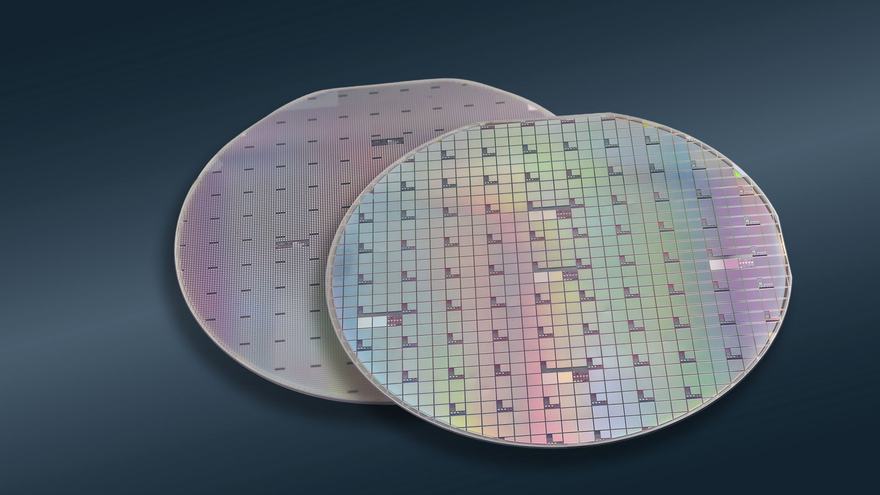
Vertical Semi also differentiates itself from other companies offering vertical GaN by taking the technology to market using an entirely CMOS-compatible approach. Following the 2025 fundraising announcement, the startup said it had already demonstrated its technology on eight-inch wafers using standard silicon CMOS semiconductor manufacturing methods.

“We made these vertical GaN devices in a CMOS fab using silicon tools, and not even state-of-the-art silicon tools, demonstrating that we can not only make this technology highly performant, but also very cost-effective and scalable.
“We are able to go to market in any CMOS tool set,” she adds, “and that could be both 200mm, which is what we're focused on right now, but also in the future for 300mm … and we think that our approach of leveraging great CMOS tools, especially ones that are somewhat out of date at the 200mm level, but making state of the art technology using them is an incredible way to really, truly scale.”
Liao goes on to note that Vertical has also added design features to its offering that have made manufacturing its hardware much more possible, with the company claiming that even its early prototypes have demonstrated performance gains.
“We are working now to scale this with a commercial foundry partner … and while we’re in the early stages, that transfer to a commercial fab will help us to bring this to market and address the data center power challenges.”
Going for GaN
That being said, the GaN-based future being promised is not without its challenges.
Although Jalabert claims that raw materials are not an issue, it should be noted that gallium is not a material that naturally occurs in a pure form. Rather, it is primarily extracted as a trace byproduct during the industrial processing of bauxite (to make aluminum) and zinc ores.
Additionally, a February 2026 report from the US Geological Survey noted that the United States has not mined any gallium domestically since 1987. And although China lifted its ban on gallium exports to the US for a 12-month period starting November 2025, the country currently accounts for 99 percent of worldwide primary low-purity gallium production.
Both Jalabert and Liao acknowledge the current geopolitical state of play. But for Vertical Semi, being a fabless chip company means the startup does not ever interface with raw gallium, instead sourcing gallium epitaxial wafers – wafers which have a layer of gallium nitride grown on the substrate via epitaxy (a type of crystal growth or material deposition).
“We take all that and bring it into a fab, and we do the processing, the design, and the packaging, all those things. So far, we have had no issues with sourcing the native materials,” Liao says.
“Because our approach specifically does not leverage bulk GaN (pure crystal wafers as opposed to GaN that has been grown on substrates like silicon or sapphire), rather we use an engineered substrate that does not have gallium nitride in it, we're not sensitive to price shocks in the raw material. There's actually very little GaN in our vertical GaN devices.
“We've done the modeling around a 1,000x or 10,000x increase in the cost of the raw material, and it has very little impact on our end or on the cost at a per-device level, just because of how little of the material there is in each of our devices.”
Meanwhile, for Jalabert and Onsemi, the biggest challenge facing the company is the epitaxy process. Not only is it a complex undertaking, but the US currently has limited epitaxy capacity, with China unsurprisingly operating the majority of facilities capable of the process.
“This is the challenge,” he says. “This is actually the secret sauce, it's what you hide from your competition – how you’re developing this technique, how to grow your GaN on top of the substrate, because everything else is very close to standard chip manufacturing.”
Despite these potential speed bumps, the road to GaN is paved with good intentions, and interest in the technology is only getting stronger, Liao claims.
“Across the board, whether that's low voltage or high voltage, I would say that as we move towards 100V DC racks and beyond, there's a big recognition that silicon carbide just isn't really sufficient for this purpose, and that's really because of the need to be able to drive, high voltage, high efficiency, and high density at the same time. None of those is less important than the other, because if you can’t do all those things at the same time, then you're having to really change how the rack is being designed.
“My hypothesis is that as technologies like ours and others become more readily available, the market will be ready to bet on the adoption of GaN. And, of course, technology rollout is always dependent on how well we can deliver a solution that meets our customers' needs, so that's what we as an industry on the GaN side need to be laser-focused on. How do we do this both well and reliably, because this is an amazing opportunity for gallium nitride to achieve the impact that it was always meant to achieve.”




Comments