It’s well known that Moore’s Law is coming to an end. We can no longer expect processor power to double every two years, as more transistors are packed onto each silicon chip.
That’s inconvenient for conventional IT, which has been riding high on the continuing dividend from Moore’s Law. It’s potentially a disaster for artificial intelligence (AI), which is on the verge of a big expansion… but an expansion that depends very much on fast processing.

One startup believes the answer is to combine conventional silicon with photonic processors that operate with light.
The AI explosion
Artificial intelligence is in a furious growth phase right now, says Nick Harris, CEO of Lightmatter: “People have found use cases that are insatiable. They will take as much as they can get, they'll spend any amount of money. Google, Microsoft, Amazon, and Facebook, will pay anything for these things.”
This is a recent development. After surges in the 1960s and 1980s, AI research was progressing slowly. Then in 2012, a neural network called AlexNet, created by Alex Krizhevsky, won an image recognition contest running on low-cost GPU hardware.
That showed commercial possibilities, Google bought Krizhevsky’s company, and investment began.
“There was this massive investment in scaling these things out,” says Harris. The investment bore fruit. “In the past ten years, the complexity of AI models has followed a 3.6 month doubling period.”
The trouble is, even cheap general-purpose silicon can’t keep up with that. And, while it’s possible to throw extra time and resources at an AI in the lab, it needs fast performance when it is deployed in real applications.
“The challenge with AI is, you can train very big models, but if you'd like to deploy them and have people interact with them, the time between a user making a query and getting a result back, is very important,” says Harris. “You need real-time feedback. The big challenge in the field is to build machines that can run these huge neural networks so you get an answer back within milliseconds.”
Silicon can’t keep up
Processor performance has been doubling every two years for decades, since 1965, when Intel’s Gordon Moore noted the trend.
That’s been good, but that rate of progress was not enough to keep up with AIs emerging this century, says Harris: “Even if you have the best case scaling for electronics, you're not really powering this.”
And to make matters worse, just at the moment smarter AIs arrived, the rate of silicon acceleration slowed.
Moore’s Law held because chip makers could double the number of transistors packed on a fragment of silicon every two years, Now, while processors are still packing more transistors, they are running hotter.
“The reason we have this heat problem is Dennard Scaling,” explains Harris. Robert Dennard invented DRAM, and observed that smaller transistors used less energy, scaling with their area: “Around 2005, that broke down.”
Today’s fast processors use 300W and upwards, and Harris says that’s heading for 1kW chips.
“We're still getting more transistors per unit area. But you can't really use them, because the cooling solution does not support you using them. The chip will burn. You need to be able to develop chips that perform more operations per Watt.”
Enter photonics
What makes chips hot is resistance. Electrical signals face resistance as electrons flow in current. By contrast, light signals don’t face the same resistance, and don’t create heat - and photons also travel faster than anything else.
For some years, advanced computer designs have tried to introduce photonics, and use “electrons for processing, photons for communication,” in the words of John Sontag, an HPE scientist (HPE is an investor in Lightmatter).
Long-distance communications use fiber optics, and those fibers now penetrate deep into the racks of data centers. “You have companies selling 100 Gig pluggable optics, and they're just now deploying 400 Gig pluggable optics. They send 400 gigabits per second of data over the optical fiber to lace together racks and things that are spatially separated.”
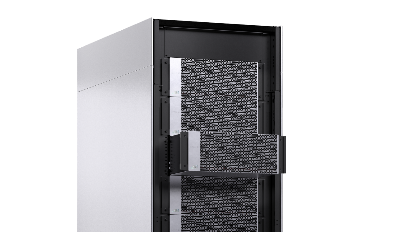
Recent developments have allowed transistors and photonics to merge on the same wafer, in so-called “co-packaged optics.” Initially, this has been seen as a way to reduce the size and power consumption of those optical plugs, bringing the signals into the chip as light, instead of converting light signals to electrical ones at the borders of the CMOS chip.
According to the roadmap, “optical components get closer and closer to the silicon until, eventually, the optics are 3D stacked and co-packaged with the processors and networking chips, giving you very high data rates at low energy consumption.”
Intel has been demonstrating co-packaged optics for a year or more, Broadcom has demonstrated a co-packaged optics switch, and Marvell bought photonics company Inphi for $10 billion in 2021, but the industry is skeptical about it coming into play quickly.
“It’s just too early to have a co-packaged optics solution that is ready for mass deployment and volume production within the next few years,” said Dell’Oro Group analyst Sameh Boujelbene in a comment to SDxCentral this year.
Co-packaged optics could be useful for making the highly-interconnected GPU systems used in training AI, but that still requires compute clusters with a “rat’s nest” of interlaced optical fibers, comments Harris. “They're planning to lace together the processors inside the server using the optics. When every chip is connected to every other chip using a fiber, there are performance benefits, but it's very hard to service those things.”
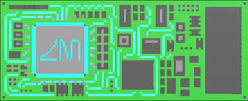
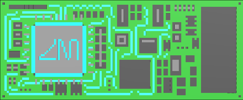
Lightmatter’s approach is to push the optical elements further inside the chip, so all those interconnections are handled by a switchable photonic network within the silicon, that generates no heat, and takes up minuscule volume.
“Fiber is macroscopic, it's on the order of a millimeter,” he says. “Our devices are two microns.”
This could drastically reduce the hardware required, effectively integrating a complex AI training system onto a single chip: “If you open our server, there's one chip in there. It contains all of the processors for the server. And they're optically interconnected inside of the chip. And they can communicate with other platforms over optics as well.”
He continues: “Ultimately, what this thing does is extreme integration, enabling everything with optical interconnect, and allowing for really absurd bandwidths.”
And it’s done in standard processes available from merchant silicon fabs: “We built our wafers with GlobalFoundries,” says Harris. “We have transistors that are very close next-door neighbors, within 100 nanometers of the photonic components. It's all monolithic.”
The same etching tools make the CMOS, and the photonic connections, which are on the same nanometer scale as transistors, he says.
“We use all the same etching tools. So it's all completely standard CMOS. We use a ‘silicon on insulator wafer,’ which is used in the production of many electronic chips.”
Harris and colleagues developed the idea at MIT, and have been commercializing it since 2018, with the aid of $11 million in startup funding.
Going to silicon
The company has two products. Passage is an interconnect which takes arrays of traditional processors and links them up, using a programmable on-chip optical network.
“Lasers are integrated into the platform, along with modulators and transistors,” he says. “If you take a scanning electron microscope to the thing, you can see the waveguides - they are spaced about two microns apart, and are a few 100 nanometers wide.”
The other product is Envise, a general purpose cloud inference accelerator, which combines computation elements, with a photonic computing core.
The promise here is to address the issue of AI processing speed: “We have about a 42x improvement in latency, because the processing is happening at the speed of light. You're doing multiplication and addition as light flies through the chip.
The technology is still at an early stage, but Harris says Lightmatter has “about five customers,” who are large enterprises. The company has silicon in the lab, and will have the chips on general availability later in 2022.
“In the Passage case, we're looking at the communication between chips, and in the Envise side, the optical processing core helps with communication energy, and also offloads computer operations,” says Harris.
The products are “big chips,” says Harris. Much like another AI chip startup, Cerebras, Lightmatter has found that integrating multiple cores and a network can be done across a single wafer.
Cerebras is further advanced commercially, with products adopted at the EPCC supercomputing center of the University of Edinburgh, and at Biopharmaceutical company AbbVie, among others. However, it has had to create its own liquid cooling system to deal with the heat generated in the on-chip network.
Lightmatter’s optical network sends signals with photons and runs cooler. It’s also somewhat smaller, but is still “inches across,” with Passage fitting into an eight-inch by eight-inch chip socket: “The biggest chip socket I've ever seen in my life.”
It does, however, offer that “absurd” bandwidth: 768Tbps.
Wafer-size chips might sound like a liability, given that all silicon wafers can suffer from small point defects, so a large wafer has a higher chance of failing. “We do a lot of work on yield engineering,” says Harris. “But there are not a lot of transistors on the chip.”
With few transistors, there’s less chance of point defects: “We have very low densities, so there's a very low probability of getting a point defect in manufacturing that kills the transistor. The yields end up being high because it's not a very densely integrated transistor circuit.”
Applications
The first applications for this will be companies that do analysis of real time videos, says Harris. These could include security firms, but also companies monitoring a manufacturing line using cameras to spot when a part has a defect.

Issue 46 - The Last Data Center
Long-term data storage enters a new epoch
It’s also potentially useful for speech analysis and other AI applications: “It's across the board.”
There’s one common factor - customers are interested in the “transformer” type neural networks pioneered by Google, and want to implement them more cheaply
“The first application would be principally trying to address dollars-per-inference cost. If you're a product person who is working on Google Cloud, there are a lot of AI models you'd like to deploy, but you can't afford to, because the dollars per inference doesn't make sense.”
Will it all work? One positive sign is the caliber of the engineers joining the company.
Richard Ho, one of the leaders of Google's custom AI chip family, the Tensor Processing Unit (TPU), joined Lightmatter in August, following Intel's VP of engineering, data center, AI group, Ritesh Jain. In May it hired Apple finance director Jessie Zhang as VP of finance.
The prospects for photonic computing could be bright.

