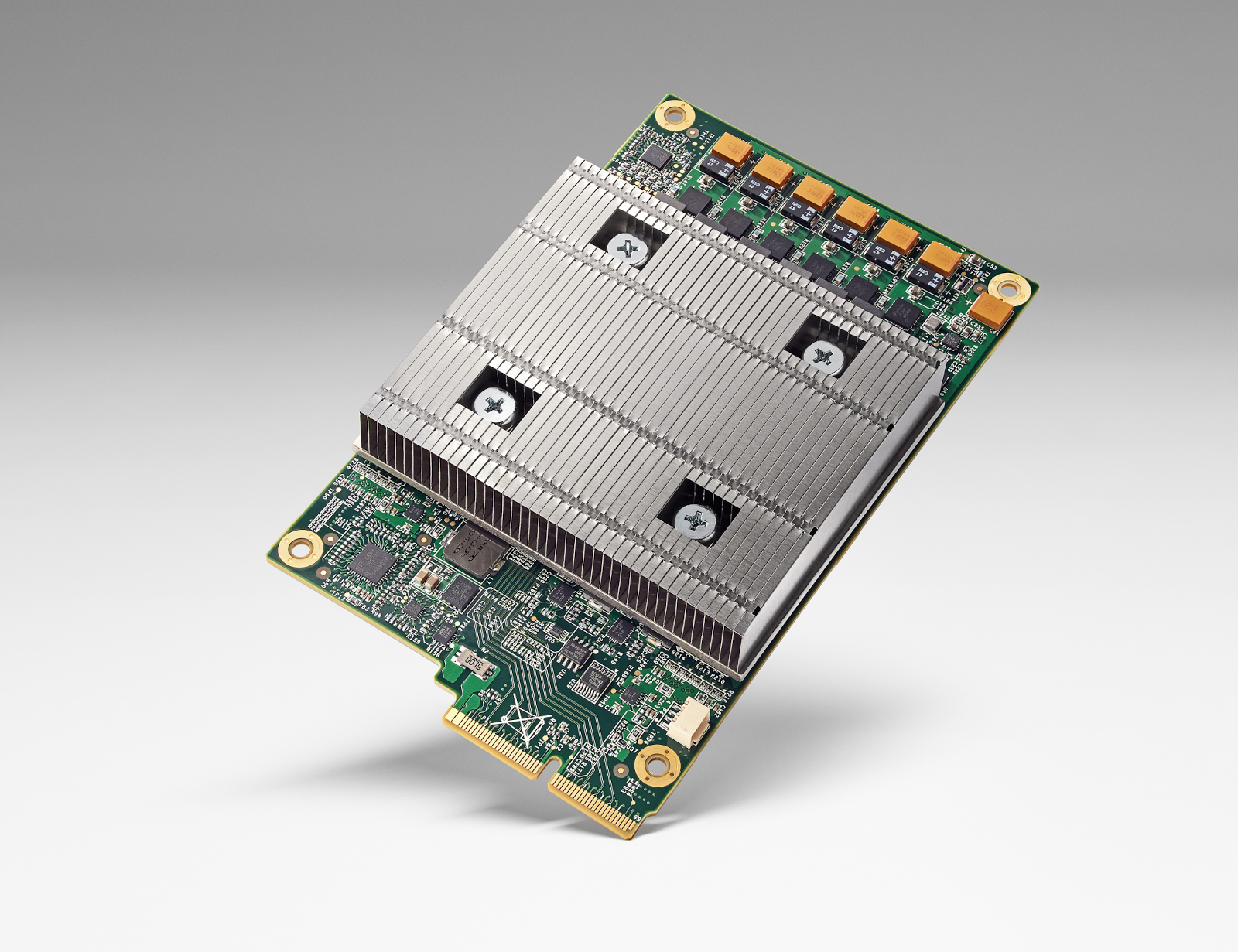
Back in 2015, Google began putting its own custom machine learning accelerator in its data centers, claiming significant improvements over off the shelf gear.
Since then, details on the Tensor Processing Unit have remained few and far between, but now the Internet giant has finally provided insight into what its chip can do.

A matter of inference
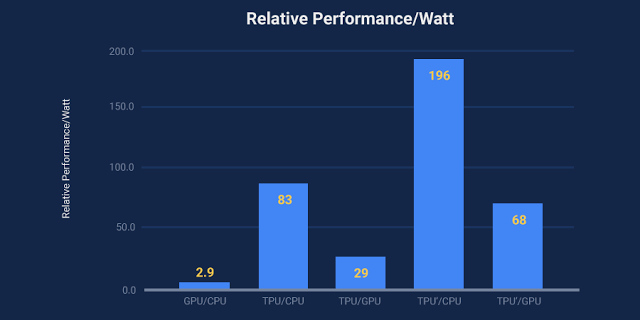
“On our production AI workloads that utilize neural network inference, the TPU is 15x to 30x faster than contemporary GPUs and CPUs,” distinguished hardware engineer Norm Jouppi said in a blog post.
Jouppi’s figure is in reference to the K80 GPU and the Haswell CPU, which are not the latest chips on the market, but are predominantly used by cloud providers in data centers. The TPU is also focused on inferencing, rather than training neural nets (executing rather than creating).
He continued: “The TPU also achieves much better energy efficiency than conventional chips, achieving 30x to 80x improvement in TOPS/Watt measure (tera-operations [trillion or 1012 operations] of computation per Watt of energy consumed).”
“The neural networks powering these applications require a surprisingly small amount of code: just 100 to 1500 lines. The code is based on TensorFlow, our popular open-source machine learning framework.”
The impetus for the TPU was a fear that if the over a billion Android users began to use Google’s voice search for just three minutes a day it would require Google to double its number of data centers.
While that level of voice use didn’t exactly come to pass, and the company has explored ways of doing more voice recognition work on phones themselves, Google pushed forward with its TPU plans.
In a paper, the company said: “We started a high-priority project to quickly produce a custom ASIC for inference (and bought off-the-shelf GPUs for training). The goal was to improve cost-performance by 10X over GPUs. Given this mandate, the TPU was designed, verified, built, and deployed in data centers in just 15 months.”
Google looked at field-programmable gate arrays (FPGAs), but ultimately decided against them, Jouppi told The Next Web.
He said: “The fundamental bargain people make with FPGAs is that they want something that is easy to change but because of the programmability and other hurdles, compared with an ASIC, there ends up being a big difference in performance and performance per watt.
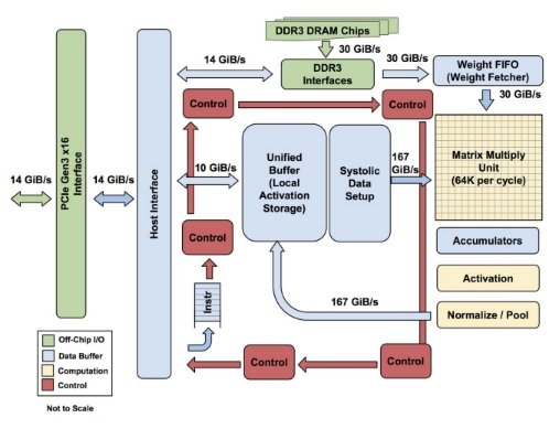
“The TPU is programmable like a CPU or GPU. It isn’t designed for just one neural network model; it executes CISC instructions on many networks (convolutional, LSTM models, and large, fully connected models). So it is still programmable, but uses a matrix as a primitive instead of a vector or scalar.”
The TPU ASIC is not the only bit of hardware Google has made for its data centers - earlier this week we took a deep dive into the company’s custom security chips named Titan, and in the past we have looked at why Google puts GPS systems in its data centers.
The company also has its own networking switches, with the ‘Pluto Switch’ being outed in 2012 when it was sent to the wrong address. Later, it gave some scant details about its Jupiter switches, before a paper delved into what Google is working on.