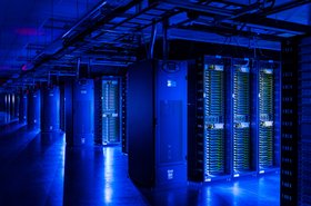
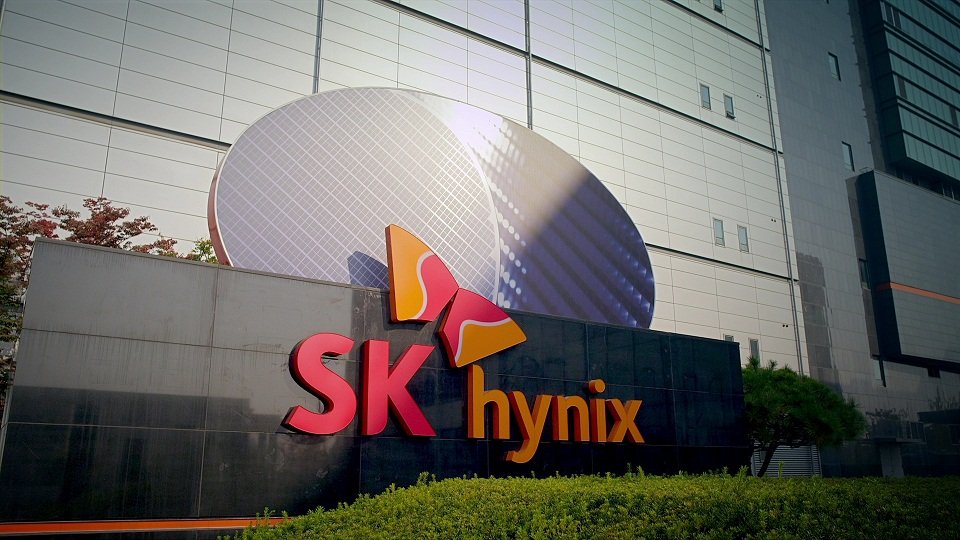
Chip maker SK Hynix is planning to make further investments in South Korea to expand and improve its advanced chip packaging technology.
According to a report in Bloomberg, the investment will be used to further advances such as lowering power consumption and improving performance to meet the growing demands of AI applications.

Speaking to the news outlet, Lee Kang-Wook, head of packaging development at the memory chip maker, said that improving that process is the reason the company’s high bandwidth memory (HBM) is in such high demand and that it is working to further cement its lead in this market.
“The first 50 years of the semiconductor industry has been about the front-end [the design and fabrication of the chips],” Lee told Bloomberg. “But the next 50 years is going to be all about the back-end [packaging].”
Using estimates from analysts, Bloomberg reported the SK Hynix investment in advanced chip packaging could sit around the $1 billion mark. However, this has not been verified as the company has not disclosed its capital expenditure budget for this year.
Lee helped develop the third generation of SK Hynix’s HBM, pioneering a novel method of packaging the technology that would become HBM2E. This led to Nvidia choosing SK Hynix to provide the HBM for the chip maker’s standard-setting AI Accelerators, a decision which has helped make SK Hynix more valuable than both Samsung Electronics and Micron Technology, its big rivals in the memory market.
In February 2024 it was reported that the company had chosen Indiana as the site of a new packaging plant. Although SK Hynix has not confirmed the reports, in 2022 SK Group Chairman Chey Tae-won met with Joe Biden and pledged that the company would invest $22 billion in US-based semiconductor, green energy, and bioscience projects.
It’s believed the new plant will specialize in stacking standard dynamic random access memory chips to create HBM ones, before they are integrated with Nvidia’s GPUs.
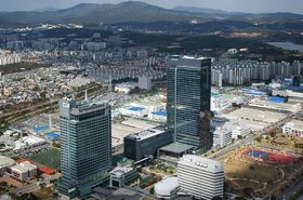
As part of the South Korean government’s plans to build the ‘world’s largest semiconductor mega cluster’ over a 23-year period, SK Hynix is also investing 122 trillion won ($91bn) in a memory production facility in Yongin, a city south of Seoul in the South Korea’s Gyeonggi Province.

