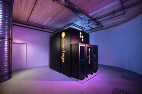
Samsung Electronics has announced it will invest $40 billion to build a semiconductor cluster across a number of locations in Texas.
The company will receive $6.4bn in direct funding under the US Chips and Science Act to support the development.

The company will receive $6.4bn in direct funding under the US Chips and Science Act to support the development.
In a statement announcing the funding, the Department of Commerce said Samsung’s venture will be split across two locations in central Texas.
Two semiconductor foundries producing 4nm and 2nm chips, an advanced packaging facility for high memory bandwidth, and a research and development facility will be constructed in the city of Taylor.
Additionally, an existing Samsung site in Austin will be expanded to support the production of fully depleted silicon-on-insulator (FD-SOI) process technologies, a process that allows for more efficient transistor control when compared to conventional bulk technologies.
The Taylor fabs are expected to be up and running by 2026 and Samsung said those facilities will use “leading-edge sustainability strategies” to promote carbon-free electricity use and conserve water resources. The facilities across both cities are expected to create at least 21,500 jobs, including 17,000 construction jobs and 4,500 manufacturing jobs.
Samsung Electronics will also partner with local educational institutions in the state, including Austin Community College, The University of Texas at Austin, Texas A&M University, and Taylor High School, to train future semiconductor workers.
Additionally, the company is looking to collaborate with the Department of Commerce to provide its employees with affordable, high-quality, and accessible child care.
“We’re not just expanding production facilities; we’re strengthening the local semiconductor ecosystem and positioning the US as a global semiconductor manufacturing destination," said Kye Hyun Kyung, president and CEO of the device solutions (DS) division at Samsung Electronics. "To meet the expected surge in demand from US customers, for future products like AI chips, our fabs will be equipped for cutting-edge process technologies and help advance the security of the US semiconductor supply chain.”
CHIPS and Science Act funding coming thick and fast
In February 2024, GlobalFoundries was awarded $1.5 billion by the US government under the act to subsidize the company’s future semiconductor production capabilities and support expansion plans for its New York and Vermont sites.
In March, it was announced that Intel would receive $8.5 billion in direct funding, $11bn in low-interest rate loans, and a 25 percent investment tax credit on up to $100 billion of Intel’s capital investments under the Act. It will be used to support the company’s investments in Arizona, New Mexico, Ohio, and Oregon where the company is expanding its chipmaking facilities.
Most recently, TSMC signed an agreement with the US government in April that would see the company receive $11.6bn under the CHIPS and Science Act to build a third fabrication plant in Phoenix, Arizona. This newly announced TSMC fab will produce 2nm or “more advanced process technologies depending on customer demand” and is expected to be in production by the end of the decade.


