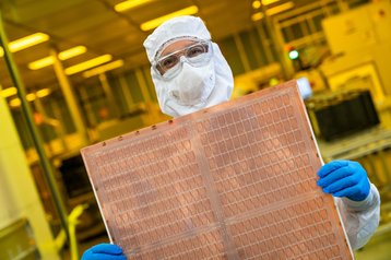
Intel has unveiled a glass core substrate for future semiconductor advanced packaging.
Expected to be ready for the end of the decade for both Intel and Intel Foundry customers, the company believes that the technology will bring multiple advances to chips, improving performance in the years to come.
Modern 'organic packages' use a woven laminate core and have served chips well for multiple generations, but Intel believes that the technology will likely reach its limits due to issues like shrinkage and warping, and less efficient power use.
Glass could support larger packages, have better thermal stability, and have ultra-low flatness for improved depth of focus for lithography. They could allow for a 10× increase in interconnect density, the company claimed.
Chips are getting larger and more complex with chiplets, and Intel believes that glass substrates will allow it to keep growing. "These many benefits bring the industry closer to being able to scale 1 trillion transistors on a package by 2030," it said.
The company has spent about $1 billion on the project to date, and has developed an electrical test chip.
“After a decade of research, Intel has achieved industry-leading glass substrates for advanced packaging," Babak Sabi, Intel SVP and GM of Assembly and Test Development, said. "We look forward to delivering these cutting-edge technologies that will benefit our key players and foundry customers for decades to come.”


