
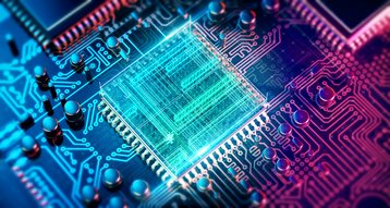
Consolidation and slowing innovation in the semiconductor market has created a landscape where today’s chips are so close in design that they are almost commoditized. However, with a growing number of product manufacturers looking to disrupt their market by pushing more varied and complex functions to the Edge, the need for innovation has never been greater.
The impact of this innovation could be vast. It’s feasible that the business case to embed complex machine learning at the Edge could evolved rapidly. This means more of your virtual assistant’s brains, for example, can be in the living room rather than in the cloud, desirable from both a performance and a privacy perspective.
Keep your friends close, keep you Edge devices closer

The Edge of the Future
A special supplement tackling the fundamental questions surrounding Edge computing. Hear from industry experts, and from DCD's readers, to learn where the Edge will live.
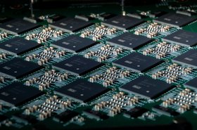
Semiconductor design for Edge devices is inherently complex, where there is often a need to include both analog (sensors, radios, etc.) and digital (compute, memory, etc.) features on the same silicon, with a mixed signal device. However, this is where physics come into conflict with economics. Under these conditions, the fundamental business principles of semiconductor chip design are no longer relevant.
Mixed signal devices are an inherent compromise, with the solution being good enough for each function, but optimal for none. This high level of integration increases development costs and chips must serve as many applications as possible to create a return on the investment. If the digital functions are to be improved to incorporate the latest machine learning architectures on smaller transistors, then much of this investment must be repeated.
Unfortunately for product manufacturers, a lot of chip functionality also goes unused, creating a needless drain on cash and power. So how do semiconductor companies break this mold and offer a feature rich silicon design that also pushes the parameters of low cost to the extreme? This not only holds the key to unlocking a wealth of new IoT applications, but can transform semiconductor companies’ own competitive advantage.
One area of innovation in low cost at the Edge concerns the disaggregation of the analogue and digital worlds. Critical aspects of analog performance are more easily achieved with larger feature sizes, to provide the high levels of accuracy and low levels of noise required. On the flip side, digital features are being increasingly developed on smaller feature sizes to reduce cost and size. Therefore, mixed signal devices commonly mean paying for a small feature size that at best conveys no benefit for the analogue functions and at worst decreases performance with a significant cost increase.
Furthermore, each time a product manufacturer or semiconductor company wants to improve the digital functionality, the entire chip, including the analogue IP, must be redesigned. It’s a time consuming and extremely costly exercise. This redesign process also brings undue risk due to the number of technologies involved in maintaining the analogue performance, in the presence of high-density digital components.
Disaggregation of the chip
Faced with this challenge, a growing number of semiconductor companies and product manufacturers are looking at ‘chiplets’ as a solution. This strategy concerns the disaggregation of functions into separate pieces of silicon.
Chiplet architecture is much like the modular approach of a PC: it has a processor board, sound card and graphics card, and you only need to change one element to upgrade. Each chiplet can be designed and fabricated to deliver optimal performance for a specific function of a specific device. Combining these functions into an edge device brings many advantages over traditional monolithic semiconductor design. Improvements in inter-chip connectivity, with reduced cost, is making chiplets economically attractive for a wider set of applications.
Firstly, only the specific functions needed for the device are included – removing the unnecessary cost and space of unused functions associated with commoditized silicon. Product variations are managed through choosing which chiplets are combined, rather than needing to alter the chip design itself. Enhancement to digital features can be done independently, significantly reducing the cost and risk of respinning an entire chip. This brings huge benefits in accelerating time to market, far outstripping any traditional approaches.
These approaches are set to fundamentally shift the economics of semiconductor design, pushing the parameters of low cost to the extreme and helping product manufacturers transform their markets with disruptive IoT.

