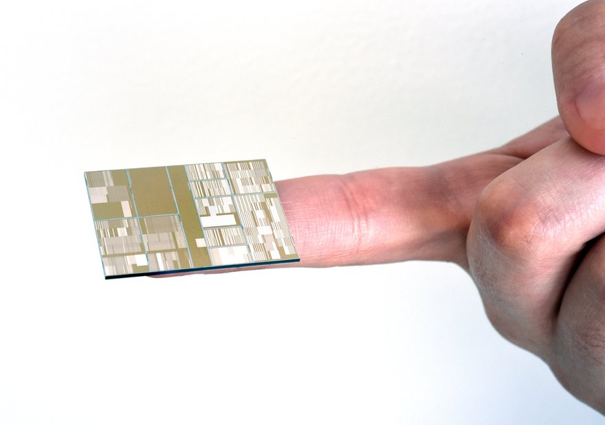
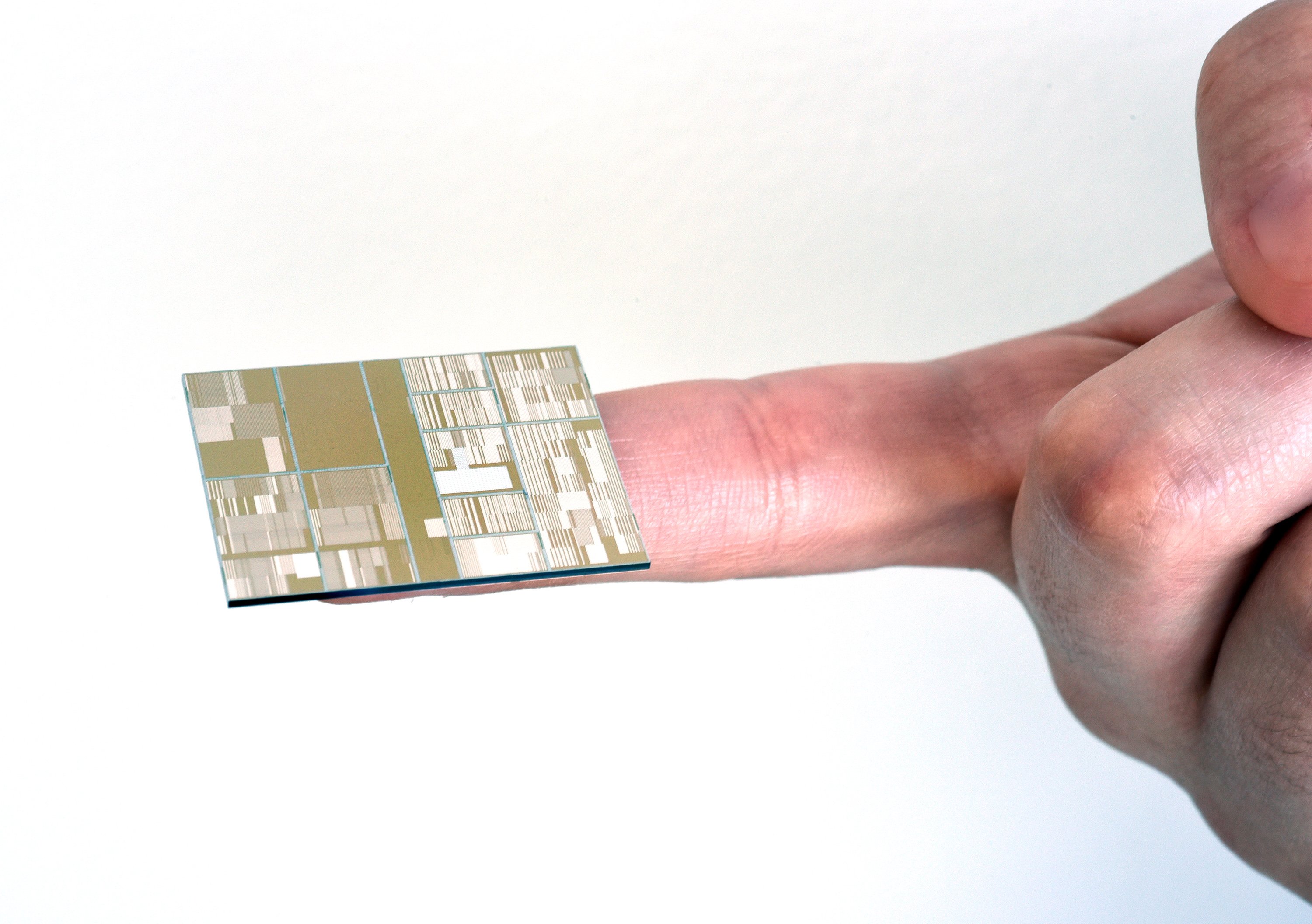
IBM Research has built the industry’s first funcitoning 7nm test chips, putting it one generation ahead of other silicon fabrication outfits.
The smallest process technology currently in use is 10nm, and to move beyond that, IBM has had to move from optical to ultra-violet light in the photo-litho production process. This in turn has necessitated changes in the chemicals used in the chip’s conducting pathways.
Still a player
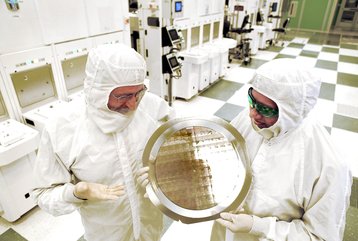
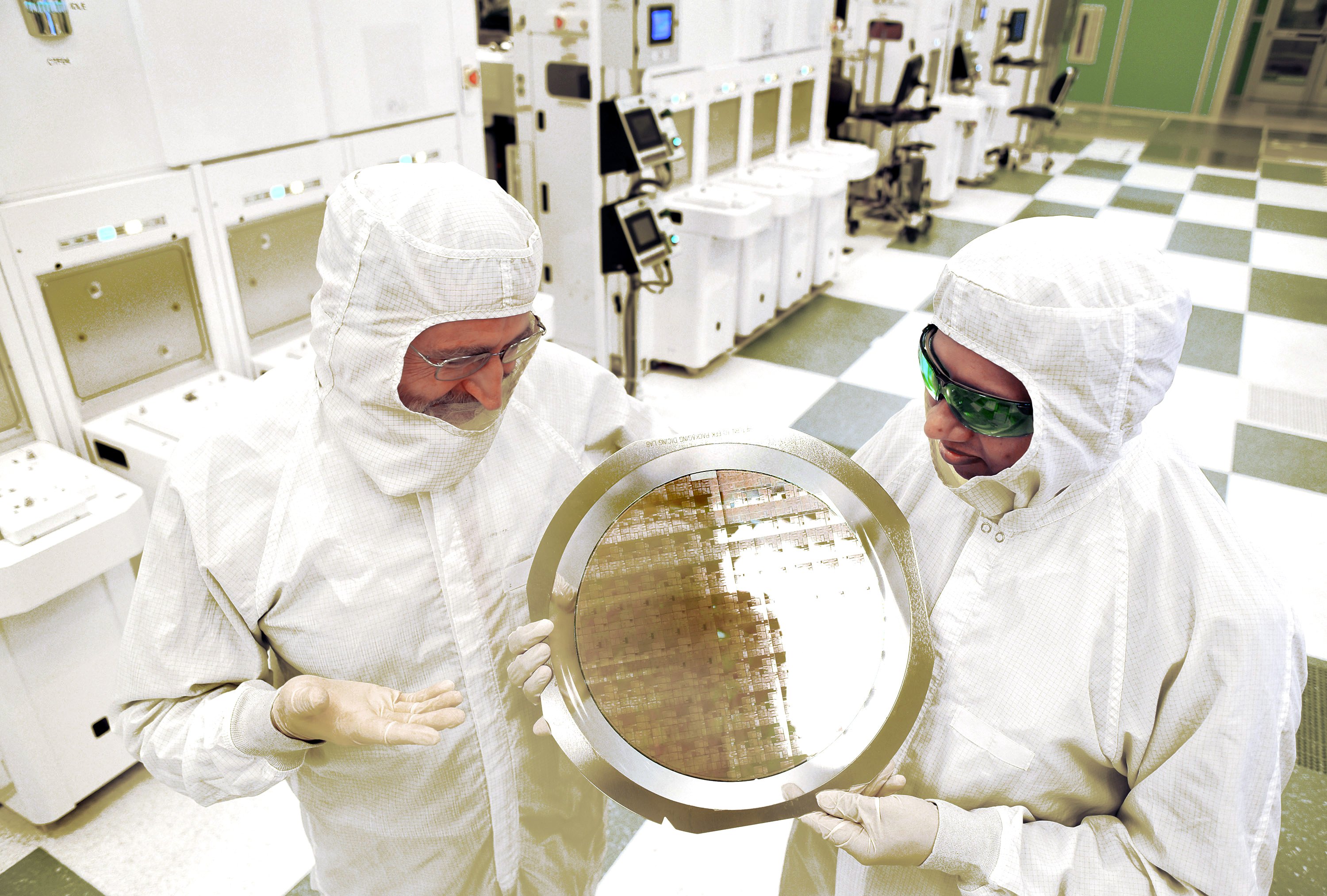
IBM sold its silicon production ability to GlobalFoundries in 2014 and became a “fabless” chip designer, relying on partners such as GlobalFoundries to make the processors it uses. But it held onto its research labs which push the fabrication process forward and continued to invest, announcing a $3 billion investment in 2014.
”Optical lithography has totally run out of steam,” said Mukesh Khare, VP, semiconductor technology for IBM Research, in an interview with DatacenterDymamics. “Extreme UV lithography is a breakthrough.”
The new process uses a wavelength of 13.5 nm, some ten times smaller than the wavelength currently used, and this necessitates new materials in the layers of the chip, which can be exposed by the UV light.
A silicon germanium (SiGe) channel material is used and the EUV process is integrated at multiple levels. The work was done with the help of New York State University’s NanotTech complex in Albany.
So far this gives IBM an improvement of 50 percent over current area scalings, but this can be pushed a lot further, said Khare. These efforts could result in at least a 50 percent power/performance improvement for the next generation of systems.
“It is harder to deal with EUV because it is a completely new method of generating light,” said Khare. This requires changes in tooling to generate the wavelength and integration into the lithorgraphy process. “We want to use as many conventional processes as possible, but we have had to create new resistor materials, that are activated by this light source, and new etch chemistries,” he told DatacenterDynamics.
The one thing he couldn’t tell us was how quickly the process will be implemented in actual products. This will be in the hands of GlobalFoundries, but you can bet that both IBM and its partner will be doing their best to maintain this head start over Intel.