
Microprocessors can now see the light. A multi-university research team has combined electronics and photonics, putting 70 million transistors and 850 optical modulators, filters, photodetectors, and couplers on to a single 3mm x 6mm chip. The disparate technologies are integrated with each other, and communicate via light with the outside world.
This is a long-awaited and much-needed breakthrough. Chip electronics are fast approaching electrical and thermal limitations (current leakage, crosstalk interference and heat build-up). Before long, electronics alone will not be enough to build more powerful microprocessors.
What’s the big deal?
Optical components do not suffer from the problems that plague electronics, but putting them on silicon is not without its challenges, because silicon does not transmit optical signals nearly as well as glass.
Research labs such as Intel’s Photonics Technology Laboratory have developed silicon-based lasers, optical modulators and photodetectors, but any recent news about silicon-photonic development has dried up. Giacomo Losio, head of technology at ProLabs and former lead optical engineer of Cisco’s transceiver module group, says that combining those components to make a working prototype could take years: “If there is a mistake in the chip design, the prototype chips are scrapped, the design changed, and the entire chip fabrication process starts over.”

But that wait could now be over. “This is a milestone. It’s the first processor that can use light to communicate with the external world,” says Vladimir Stojanović, associate professor of electrical engineering and computer sciences at the University of California, Berkeley, in a press release. “No other processor has the photonic I/O in the chip.”
The team also includes fellow UC Berkeley professor Krste Asanović, Rajeev Ram at the Massachusetts Institute of Technology, and Miloš Popović at the University of Colorado, Boulder. “This is the first time we’ve put a system together at such scale, and have it do something useful, like run a program,” adds Asanović, who designed the instruction set architecture (RISC-V).
But the research team didn’t just design the first-ever electronic-photonic chip system. They circumvented custom manufacturing processes, designing on-chip photonic components to be fabricated using standard microprocessor foundry technology.
The single-chip photonic-electronic microprocessor
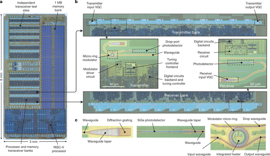
The above slide shows the die photo of the 3 mm by 6 mm chip with the processor, memory, and transceiver banks called out (a). The processor transmitter and receiver banks (identical optics) with close-ups of the individual transmitter and receiver sites (b). The lower right images are micrographs of the grating coupler, photodetector, and micro-ring modulator (c).
One of the team’s key innovations was getting optical signals to move though silicon with minimal loss. “The researchers used the silicon body of the transistor as a waveguide for the light,” says the press release. “They did this by using available masks in the fabrication process to manipulate doping, which is the process used to form different parts of transistors,” it states.

Next, the team managed to modulate the optical signal. “They designed a silicon ring with p-n doped junction spokes next to the silicon waveguide to enable fast and low-energy modulation of light,” explains Stojanović.
They also used existing silicon-germanium processes to build a photodetector, using germanium’s ability to absorb light and convert it to electricity. The last hurdle was talking to the outside world using optical signals. The research team built a vertical grating coupler using the chip’s existing poly-silicon and silicon layers.
The test bed
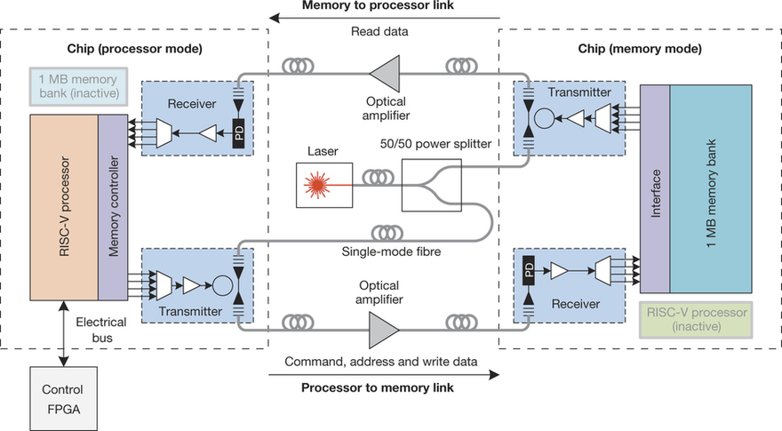
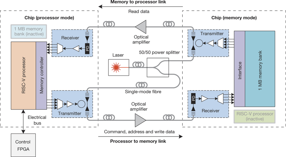
The above schematic depicts the researcher’s test bed (YouTube video). Identical chips were used. One acting as the microprocessor (left side) and the other as the remote 1 MB memory bank (right side). In the middle of the schematic is the laser power source that provided unmodulated light to the optical transmitters in each chip.
One advantage of optical transmissions is that the same amount of power is used to send the signal a few centimeters, or a few kilometers. “For high-speed electrical links, one meter is about the limit before you need repeaters to regenerate the electrical signal, and that quickly increases the amount of power needed,” says study co-lead author Chen Sun. “For an electrical signal to travel one kilometer, you would need thousands of picojoules for each bit.”
When asked what’s next for the research team, Stojanović said it will be commercialized by an outfit called Ayar Labs, and ultimately ported into bulk CMOS.
The team is not done researching either. “From a systems perspective, we’re starting to look at how this photonic interconnect can help change the switching architecture of the data center, not just get more bandwidth and less energy per existing link,” he explained.
Predictions
Losio thinks this changes things well beyond chip architecture, by allowing hardware designers more freedom: “Devices that handle huge amounts of information, almost always need a memory, and given the limitations of copper interconnects, these components need to be placed close by,” he says. “With optical interconnects, we could envision systems sharing a large memory pool located elsewhere.”
It should also help data centers go green. “Since moving data in the optical domain takes less power, and large data centers host thousands, maybe tens of thousands of servers, it is easy to see how this development could save a lot of money on the electric bill,” says Losio.
“We feel strongly that this is truly a game-changer technology,” writes Stojanović. “We’re talking here about the introduction of a major capability into an advanced process node, without any process development or any additional cost.”
If he’s right, the future looks bright for electronic-photonic chip systems.