In the history of computer architecture great designs inevitably run up against the constraints of the laws of physics. Over the last decade, high-performance computing has benefitted hugely from architects being able to leverage the scalability of CPUs designed originally for PCs. But that scalability ran up against a problem - put too many commercial-off-the-shelf CPUs together, and they get too hot.
For Intel to ford this physical chasm, it has had to throw away its old designs and start afresh. Two years ago, it unveiled its Xeon Phi class processors, substituting for the one-time seemingly infinite scalability of Core Microarchitecture CPUs with the convergence of dozens of Pentiums onto a single die. The Knights Corner generation of Xeon Phi used 22nm lithography to produce a co-processor card on a PCIe bus interface, looking something like an old Pentium Pro.
Last November, Intel previewed its second-generation Xeon Phi, called Knights Landing. This time, it was a full-scale CPU, shrunken even further by virtue of 14nm lithography.
That preview left the answer to an extremely important question hanging in the air - how would so much compute power in so dense a configuration manage memory accesses without bottlenecking?
So close, yet so far
“The gap started to widen in terms of how we were scaling our memory performance,” said Mike Black, a technology strategist with Micron Technology, in an interview with Datacenter Dynamics. “It then became such a gap that system designers were doing things creatively to get more memory bandwidth into the system. But the fundamental problem was, these multicore processors were not having access to enough near memory to allow them to operate optimally.”
Since November, we’ve known that memory would have to take a completely new form — something Intel was calling a “hybrid cube” — but we haven’t known just what form that would take.
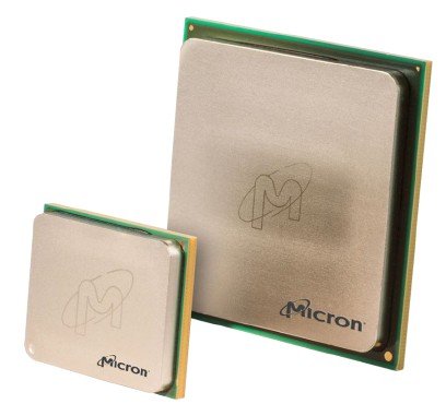
Today, at least some of the details are revealed. Once again, Intel has teamed with its long-time memory partner, Micron, to present a different, though perhaps not altogether novel, manufacturing and packaging apparatus for HPC memory. It’s still called the hybrid memory cube (HMC), which is the name that escaped from Intel’s lips during its first demonstration of Xeon Phi chips at IDF 2011.
Now, Intel officials reveal in an exclusive interview with Datacenter Dynamics, we know why it’s “hybrid” and why it’s a “cube.”
Knights Landing is based around a very dense assembly of processors — essentially, multicore without all the stacking. But you can’t exactly “multicore” your DRAM. So while multicore processors have become orders of magnitude more capable at handling and even organizing processes than their dual-core predecessors, DDRAM modules that were only four, five, maybe six times faster than before, were becoming bottlenecks.
Mike Black, Micron, said: “From a memory manufacturing standpoint, one of the challenges we face, as we continue to scale, is managing memory below 30nm. We’re running into other areas where scaling further below that is becoming more challenging. We coined the phrase ‘memory wall’ for what was preventing these multicore processors from running optimally.”
The end of memory stacking
Supercomputers built to tackle some of the world’s fundamental problems, including climate change, genetic analysis, and the energy supply, started bogging down as the scalability of those tasks into multiple threads increased. The performance gains achieved by upwardly scaling processors were not being matched by linearly stacked memory.
“Traditionally, we’ve stacked memories, but we all just used traditional wire bonding. So we were limited in terms of how many memories we could stack onto each other, by how long we could run wire bonds up the side of the package to connect to them.”
“Stacked” memory isn’t really the proper word. Wire bonding actually forms a chain. So no matter how you arrange the memory components in space, the addressability of those components was limited by the length of the wire connecting the links of the chain.
As Micron’s Black tells us, engineers could imagine the solution conceptually, but for years had no way to implement it physically. Imagine truly stacked memory along an axis, where the connecting wire runs parallel to the axis of the stack. It’s something Micron calls a thru-silicon via — a passageway through a memory stack, literally through a new and unexplored dimension.
The mistake Intel won’t make again
When Intel has faced the problem of having to cut a completely new channel for itself and prevaricated, it has paid a heavy price. In 2005, when Intel first implemented “hyperthreading” — enabling a single core to flip back-and-forth between two threads — it encountered a bottleneck. Intel’s biggest competitor at the time, AMD, capitalized upon Intel’s predicament by creating a new memory architecture called DirectConnect, that relied on embedding the controller onto the same die as the CPU.
Until it could completely re-innovate the way it fabricated CPUs, and making memory controllers native to those CPUs, Intel found itself behind the 8-ball. Though experts no longer consider AMD the competitor it once was Intel can’t afford to leave the door open to any new competitor.
So as Micron warns, engineers can’t afford to let the laws of physics rule the day. To cross this particular chasm, Micron is firstly moving the memory controller off of the CPU, and back into the memory module. Then, for Intel’s Knights Landing generation of Xeon Phi, Micron is stationing 16 GB of RAM — not cache-level memory, but dynamic memory — in a cluster-like configuration that is tightly coupled to the CPU, sharing the same package.
Put another way, Knights Landing still has the memory controller on the CPU package, just not the CPU die. This gives the processor one less thing to do; rather than coordinating how each core accesses memory by way of its native controller, the CPU can “outsource” the job to a new controller that is native to memory. This style of access lends itself to new processor designs, Black says, such as multi-pipeline systems inspired by graphics processors.
The new HMC arrangement meets Intel’s goal of quintupling memory bandwidth over traditional DDR4, and 15 times the bandwidth of DDR3, in a package that’s twice as dense using one-third of the energy. For Micron’s own part, HMC enables the company to build memory components that are 90% smaller than its current RDIMM modules, using as much as 70% less energy. Micron says it will begin shipping HMC modules in 2 GB and 4 GB packages later this year.
This week, a Knights Landing-based supercomputer built by Cray for the US Departent of Energy could land at or near the top spot in the semi-annual Top 500 supercomputers list. At that time, we’ll get our first hard evidence of the extent of the performance gains attained through Intel’s and Micron’s latest partnership.