It costs more to cool a server in the datacenter over its service lifetime than it does to power that server, or to have purchased it in the first place. For the promises of cloud computing to be fully realized before they crash into the laws of physics, materials science must enable significant improvements in our ability to construct machines on the smallest conceivable scale — one which we are just now barely beginning to understand, let alone master.
Although substantially more money will be spent on this endeavor before the goal of mass production will be finally realized, late Wednesday afternoon, IBM announced it is funding the next stage of research into graphene semiconductors, to the amount of $3bn over five years. Two years after having produced experimental transistors at the 9 nm scale using carbon nanotubes, IBM is focusing its new goal down to 7 nm by 2020.
Small is cool
At this scale, where the thicknesses of atoms are things you can measure, lesser power is literally smaller power. The only way you can make machines at this scale use less power (and transistors are, after all, machines) is to make them smaller. Graphene — a single-atom-thick sheet of perfectly bonded carbon atoms, twisted into a tube like a tortilla — is as small a conductor as is presently attainable. If fabricators like IBM can get past the problem of automating the lithography of semiconductors using graphene tubes, because carbon is cheap and graphene design is so rudimentarily simple, not many other obstacles stand in the way of mass production.
The biggest problem right now is that graphene is so weird. Imagine something that adheres to almost nothing, like a translucent jelly, except that it’s two orders of magnitude stronger than steel. Graphene has magnificent conductivity, with signal carrying capacity unlike any other material yet synthesized. Yet you can’t get it to stick to anything — certainly not the silicon carbide substrate; and not the usual fabrication metals like palladium, gold, and aluminum. You can’t glue anything to it, because at that level, there is just no such thing as glue.
Graphene parts may be held in place… in a sense, the way a tent holds down campers, but not permanently. So when an electron beam etches the wafer and a piece of graphene sticks out like a dog’s ear, it could get chopped off.
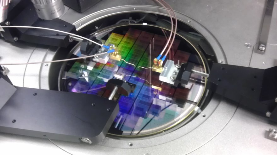
Cooking channels
Semiconductor lithography is like 3D printing except partly in reverse, by building some parts down instead of up, and depositing materials into the built-down parts in an exact pattern, like connect-the-dots. Right now, graphene nanotubes cooperate about as predictably as spirals of razor wire did during the era of trench warfare.
IBM Research succeeded in building its first graphene-inclusive integrated circuit in June 2011, but the process was described by research fellow Shu-Jen Han as something akin to cooking while blindfolded. The IC came out of the oven, if you will, and it did its job — it received and reproduced a 4.3 GHz signal without distortion, for a time — and then, well, fell apart.
Whereas a general purpose semiconductor utilizes millions of transistors, this prototype contained three, along with four inductors, two capacitors, and two resistors. It was a home electronics experiment kit, only the kit was a few microns thick.
What the $3 billion investment and the five-year mission timeline does for IBM Research is to create a ‘space race’ a formal itinerary for doing battle with cold-war adversary Intel. Like a certain space race opponent of a half-century ago, Intel boasts of having the goods, including plenty of graphene tubes to go around, except all its photographic evidence right now is top secret.
Qubits and “Moore’s Law”
When IBM is inevitably asked the question, “What will this all lead to?” in recent days its answer has come in the form of boilerplate text about so-called quantum computer components. The idea there (skipping the boilerplate nonsense) is that a new form of state container replacing the binary digit “bit,” called the qubit and made of graphene, could conceivably hold 2n electrical states rather than 21, where n is an undetermined value.
Qubit-based memory may still be years away, because its basic operating principles would be as different from everyday processors as a nuclear reactor is from a cotton gin. But the reason the qubit holds out hope for IBM researchers is because, if it were truly feasible to manipulate what physicists call “quantum dots” to produce n different states, then memory itself could become radically miniaturized.
A far simpler, smaller machine could replace today’s DRAM, and that simpler machine would be easier to fabricate using graphene than a merely reduced form of DRAM.
More accurately stated, it’s not so much that better graphene fabrication processes could lead to quantum computers, as quantum computers could lead to better graphene processes. Either way, the prospects remain bright for a potentially new form of silicon lithography and semiconductor fabrication.
Now, I know what you’re thinking. I know because we’ve all been conditioned this way: If IBM succeeds, will “Moore’s Law” be saved? I’m not entirely sure what interest IBM may have in rescuing an observation made by the founder of Intel. Nevertheless, Gordon Moore once observed that the density of transistors in integrated circuits doubles every two years. A number of variations on that theme have been declared, by Intel and others, but that’s the basic law.
If IBM’s and Intel’s race to master the graphene eventually pays dividends, then at that level, the answer to the big question will actually be, no. Moore’s Law would be crushed by a revolution in the adaptability of single transistors, enabling fewer components to do greater work.